Why TSMC Teamed Up With GlobalFoundries: Silicon Interposers and CoWoS Explained
Key takeaways
- GlobalFoundries will make CoWoS silicon interposers for TSMC under a $2 billion, five-year deal
- Production is in Malta, New York, with volume ramping in the first half of 2028
- Interposers link GPUs and HBM; their huge size makes them hard to manufacture
In AI chips, how quickly and reliably you connect HBM matters as much as GPU performance. Even a great chip can’t ship in volume if packaging can’t keep up. One key part in that process is the silicon interposer.
TSMC recently signed a $2 billion manufacturing deal with GlobalFoundries. The deal turns two former foundry rivals into partners, and it centers on that one part.
The $2 billion TSMC-GlobalFoundries deal
On Oct. 8, 2026, GlobalFoundries announced a $2 billion silicon interposer manufacturing agreement with TSMC. The initial term is five years, with plans to expand capacity as demand grows.
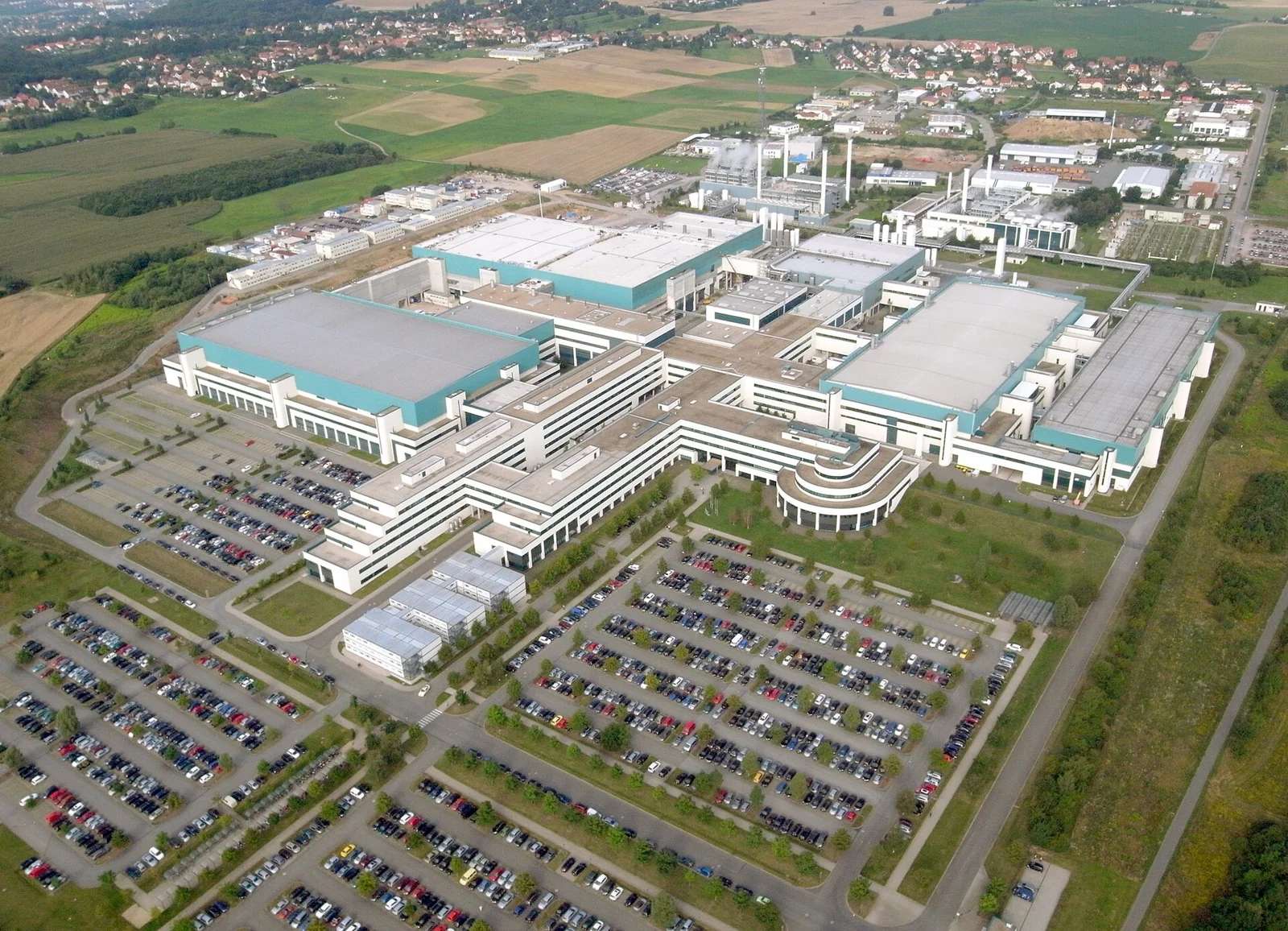
Production will take place at GlobalFoundries’ Fab 8 in Malta, New York. The fab will make silicon interposers used in CoWoS, TSMC’s advanced packaging technology.
| Item | Details |
|---|---|
| Deal size | $2 billion |
| Term | Initial 5 years |
| Site | Fab 8, Malta, New York |
| Product | Silicon interposers for CoWoS |
| Key technologies | TSV, eDTC |
| Volume ramp | First half of 2028 |
| Arrangement | Contract manufacturing of silicon interposers |
GlobalFoundries won’t assemble whole AI chips. Its job is to make the silicon interposers that connect GPUs and HBM and supply them to TSMC.
The deal gives TSMC another interposer supplier and lets it source a part needed for CoWoS packaging in the US.
The silicon interposer: linking GPU and HBM
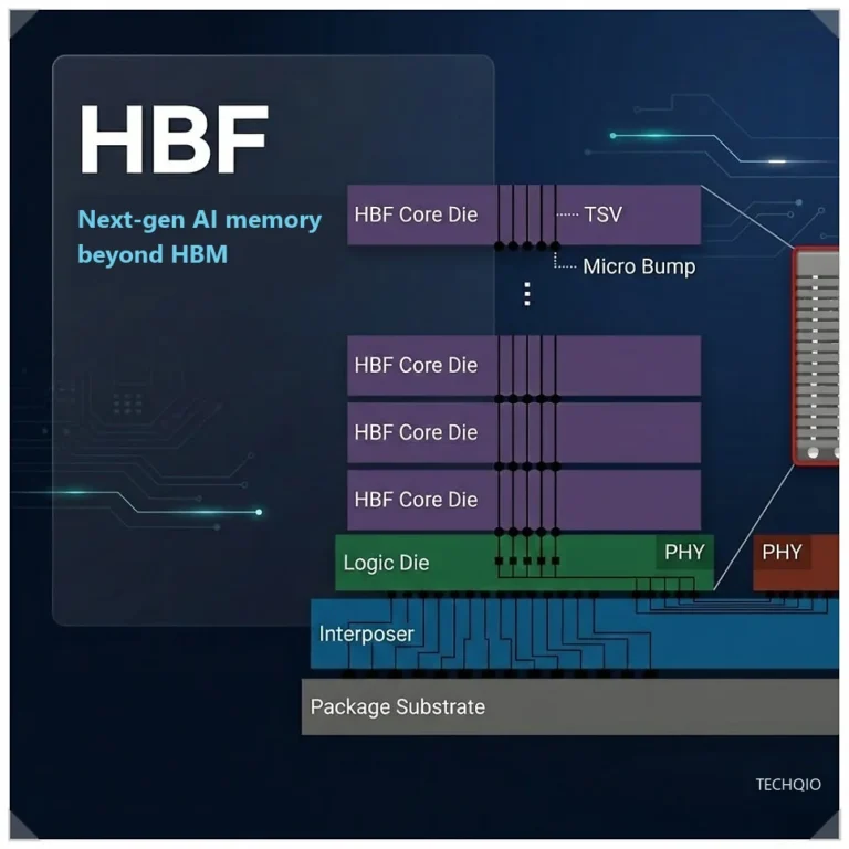
AI accelerators need more than compute chips like GPUs. They also need HBM, high-bandwidth memory that moves huge amounts of data quickly. If the link between the two is too slow, the GPU can’t be used to its full potential.
A single HBM stack uses more than 1,000 data signal lines. When the latest AI accelerators carry eight or 12 HBM stacks, the number of lines to connect grows accordingly.
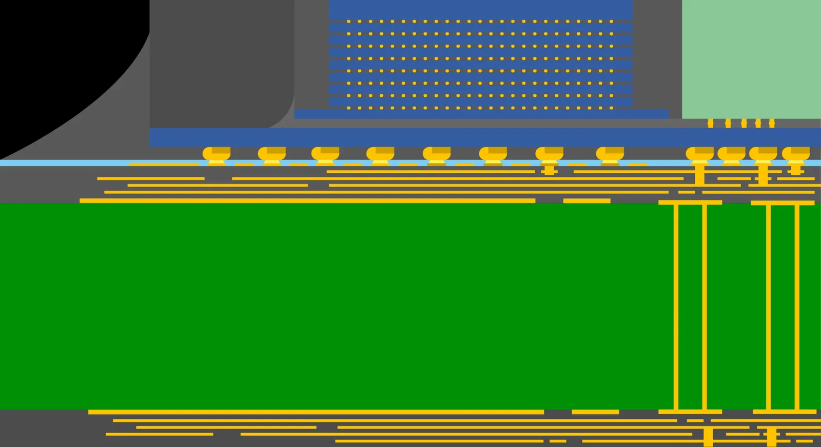
A standard organic package substrate alone can’t fit that many lines into such a small space. Longer wiring delays signals and can raise power consumption.
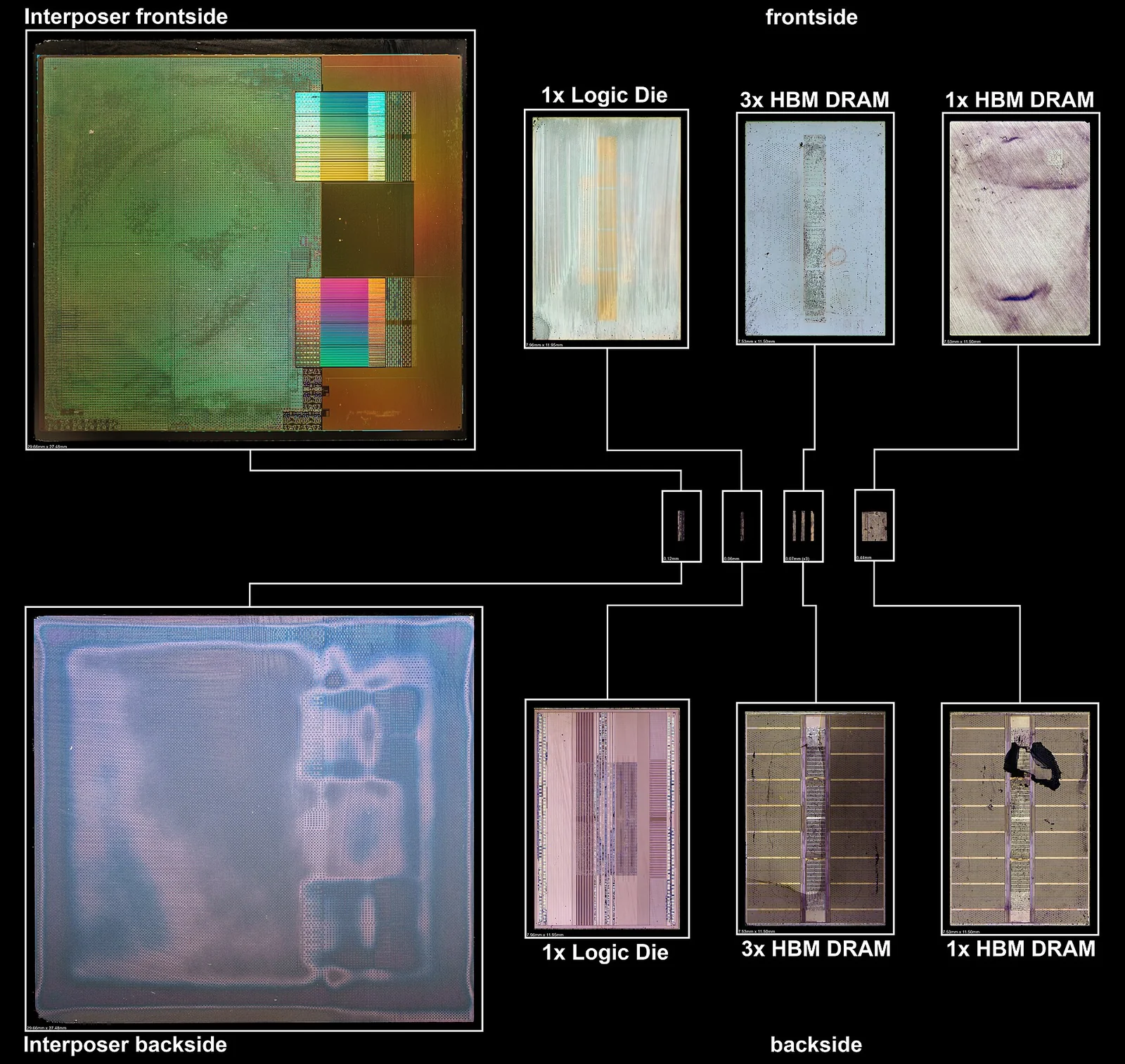
A silicon interposer is a thin slab of silicon that sits under the GPU and HBM. Chipmaking processes etch dense, fine wiring into it, so several chips can exchange data over very short distances.
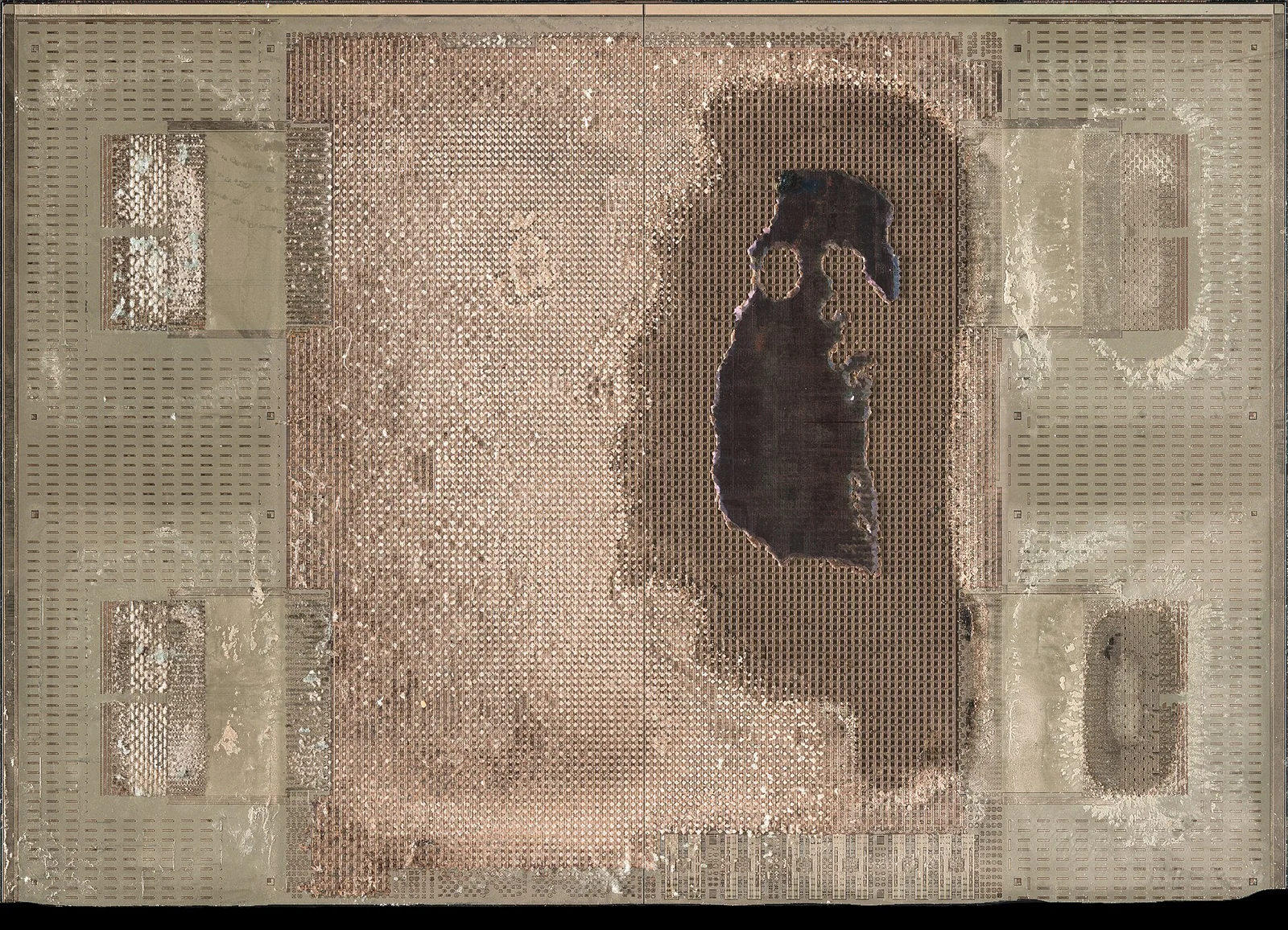
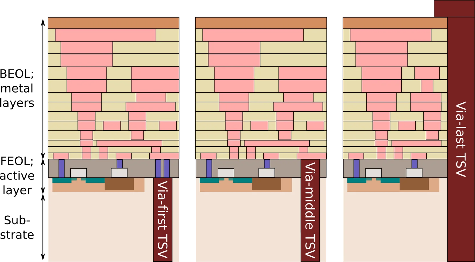
Because it expands with heat much like the silicon chips on top of it, it also eases stress on the connections as temperatures change. Through-silicon vias (TSVs), vertical electrodes that pass through the interposer, connect it electrically to the package substrate below.
The eDTC (embedded deep trench capacitor) included in this deal is a capacitor formed by etching deep, narrow trenches into the silicon. It damps voltage swings when the GPU suddenly draws a lot of power, helping keep the power supply stable.
Why silicon interposers are hard to make
A silicon interposer doesn’t do any computing, but it isn’t easy to manufacture. It needs fine wiring across a much larger area than a typical chip.
A lithography tool can pattern only a limited area in one exposure. That’s called the reticle limit, and it’s usually around 800 square millimeters.
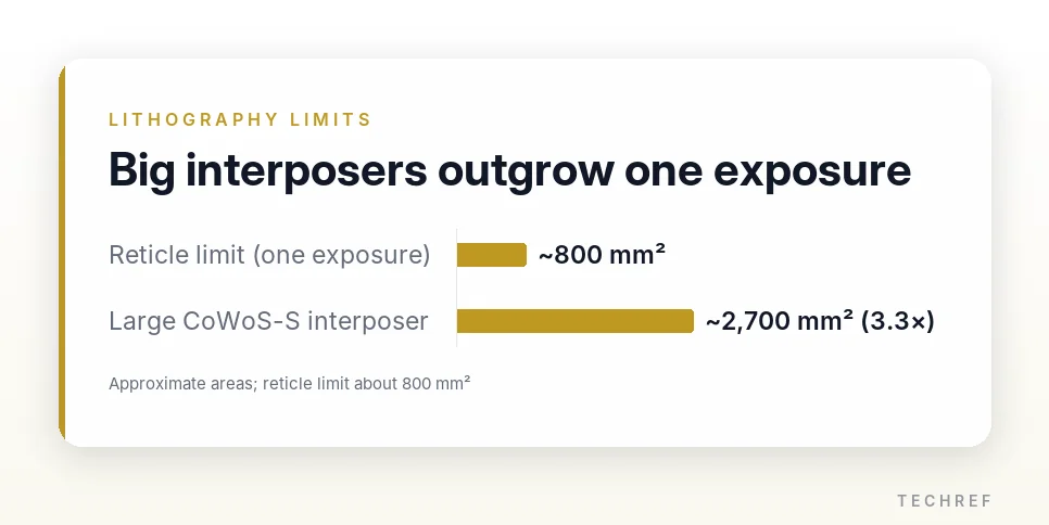
The large interposers used in TSMC’s CoWoS-S have grown to about 2,700 square millimeters, roughly 3.3 times that limit. That’s too big to pattern all the wiring in a single exposure.
The fix is stitching. The large area is split into sections that are patterned separately, and the wiring at the boundaries is made to line up precisely.
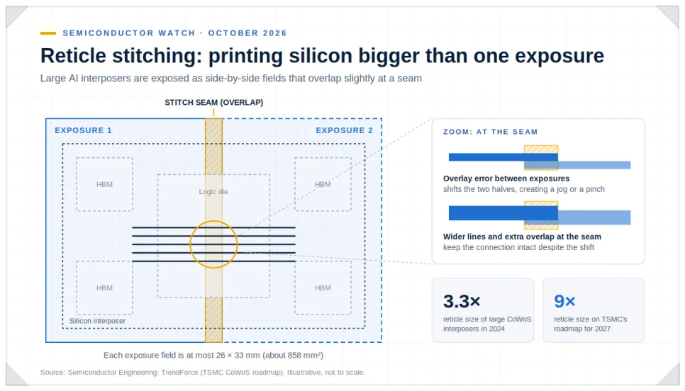
Even a slight misalignment can break connections. A defect in one section can make the whole interposer unusable. TSV processing and fine wiring add to the challenge of managing yield.
It doesn’t need a cutting-edge 3nm process. What matters is the technology and equipment to make fine wiring precisely over a large area and mass-produce it at consistent quality.
Why the former rivals teamed up
GlobalFoundries once competed with TSMC in leading-edge chipmaking. But after it stopped developing a 7nm process in 2018, it focused on mature nodes and specialty technologies.
As its strategy shifted, it overlapped less with TSMC’s leading-edge logic business. TSMC can use GlobalFoundries’ fabs to add interposer supply, and GlobalFoundries gets a new revenue opportunity in AI chip packaging.

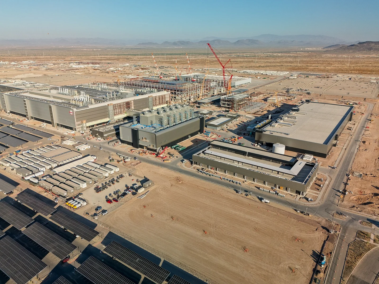
It also ties into the push to expand the US chip supply chain. TSMC is ramping leading-edge logic production in Arizona, and Amkor Technology is planning an advanced packaging facility there too.
Making interposers in Malta, New York, makes it easier to pair US-made compute chips with local packaging. Not every material and step will happen in the US, but part of a process concentrated in Taiwan can be spread out.
CoWoS-S vs. CoWoS-L vs. CoWoS-R
TSMC’s CoWoS (Chip on Wafer on Substrate) connects multiple chips into a single package. It comes in CoWoS-S, CoWoS-L and CoWoS-R, depending on how the chips are connected.
| Type | Connection | Key traits |
|---|---|---|
| CoWoS-S | Silicon interposer | High wiring density; large area is hard to make |
| CoWoS-L | Redistribution layer + silicon bridges | Easier to scale to large packages |
| CoWoS-R | Polymer-based RDL | Lower cost; lower wiring density |
CoWoS-S places the GPU and HBM on a large silicon interposer. It allows very dense wiring, but the bigger the interposer, the higher the cost and the harder it is to manage yield.
CoWoS-L uses small silicon bridges only where connections are needed. There’s no need for one huge silicon slab, which makes it easier to scale up package size. The trade-off is precisely assembling different connection structures.
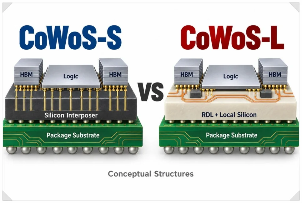
CoWoS-R uses a polymer-based redistribution layer (RDL) instead of silicon. It helps lower manufacturing costs but can’t match the fine wiring of a silicon interposer.
TSMC uses several CoWoS variants because each product needs a different mix of wiring density, package size and cost.
Bottom line: real supply gains start in 2028
Volume output from New York is still more than a year away, so it won’t ease today’s AI chip shortage right away. Even with more interposers, bonding equipment for attaching GPUs and HBM, plus package assembly and test capacity, all have to grow before shipments actually rise.
With this deal, TSMC widens its interposer supply and GlobalFoundries enters AI chip packaging. The next tests are how much US production capacity grows and how CoWoS technology evolves.