Samsung zHBM: Stacking Memory on the Chip to Break AI’s Memory Wall
Key takeaways
- Samsung zHBM stacks DRAM directly on the AI accelerator instead of beside it.
- Samsung claims about 8x HBM5 performance; its keynote slide shows 4-8x per GPU versus HBM4 and HBM4E.
- Samsung shows the 3D approach as a mockup; no production date or customer has been announced.
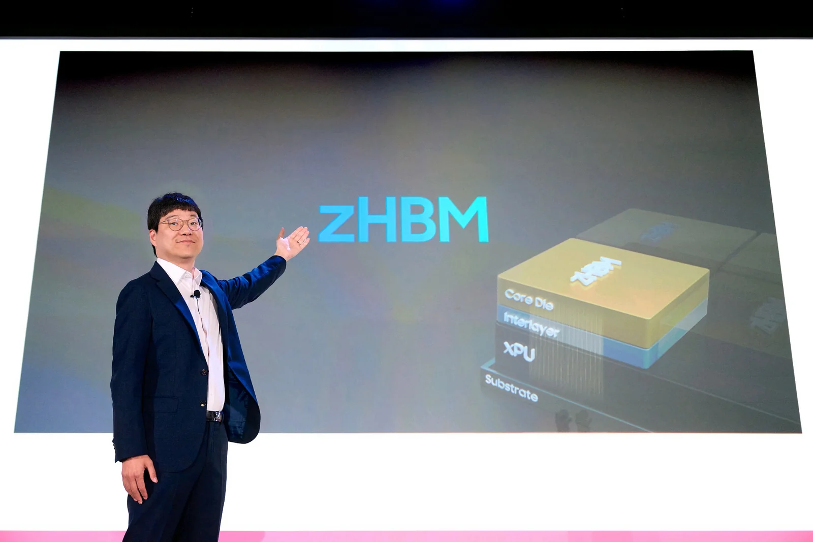
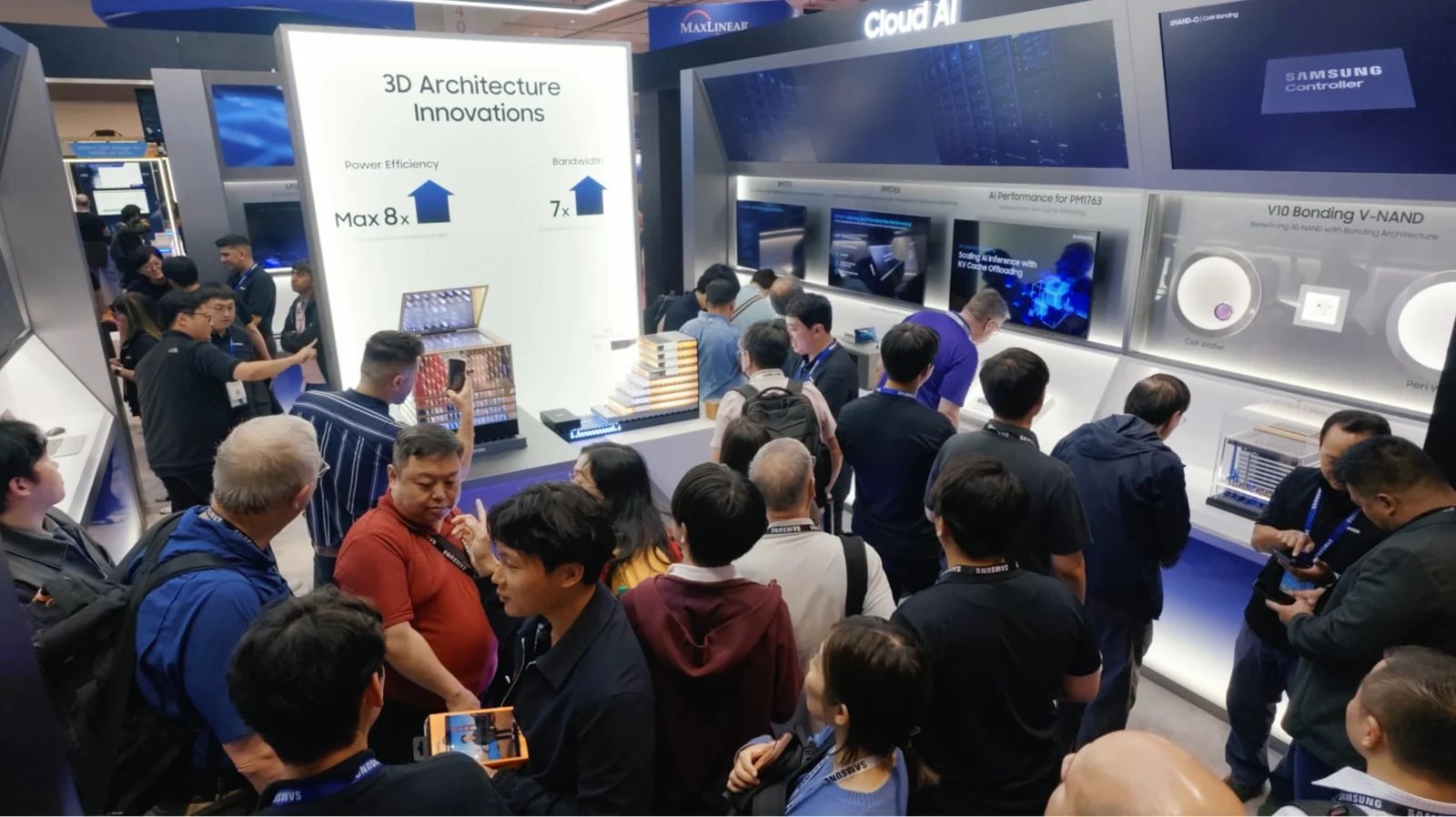
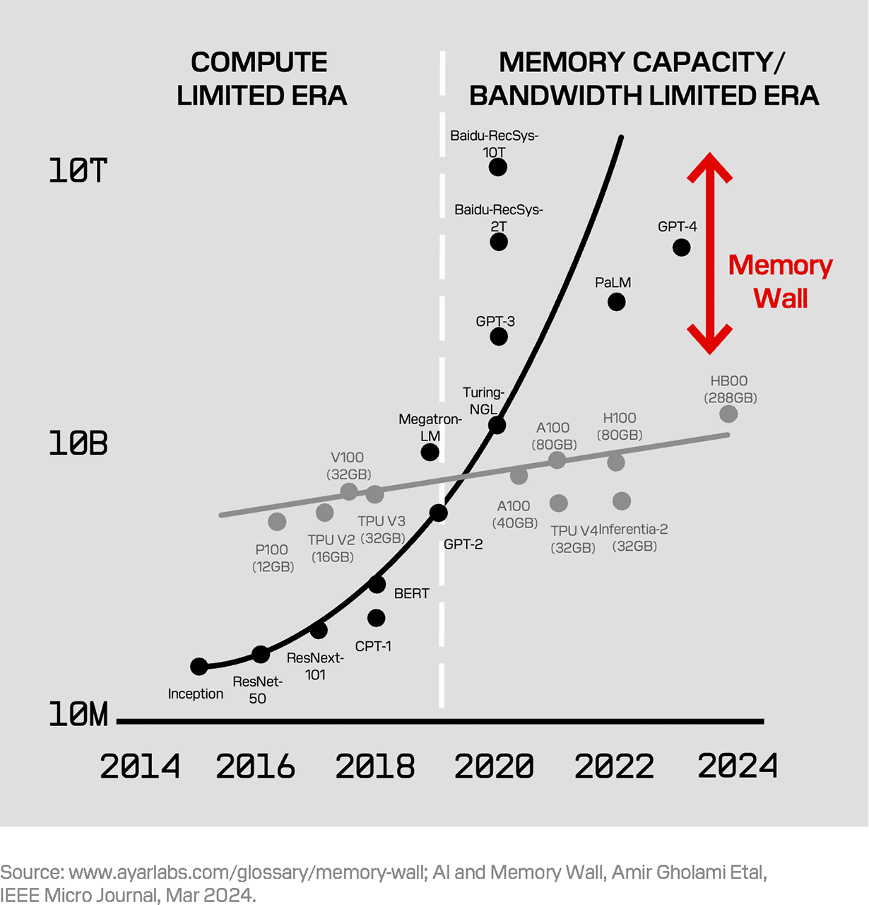
Samsung zHBM stacks DRAM directly on top of an AI accelerator instead of beside it, and Samsung showed it as a mockup at FMS (Future of Memory and Storage) 2026 at the Santa Clara Convention Center. The target is the memory wall: compute has grown far faster than data movement, so a system can only run as fast as memory can feed it data.
Moving memory from the side of the compute chip to its top makes zHBM a 3D memory architecture rather than another HBM generation. The approach changes how the chip and its memory connect, and it leaves heat, yield and ecosystem problems to solve before it ships.
The memory wall behind AI chips
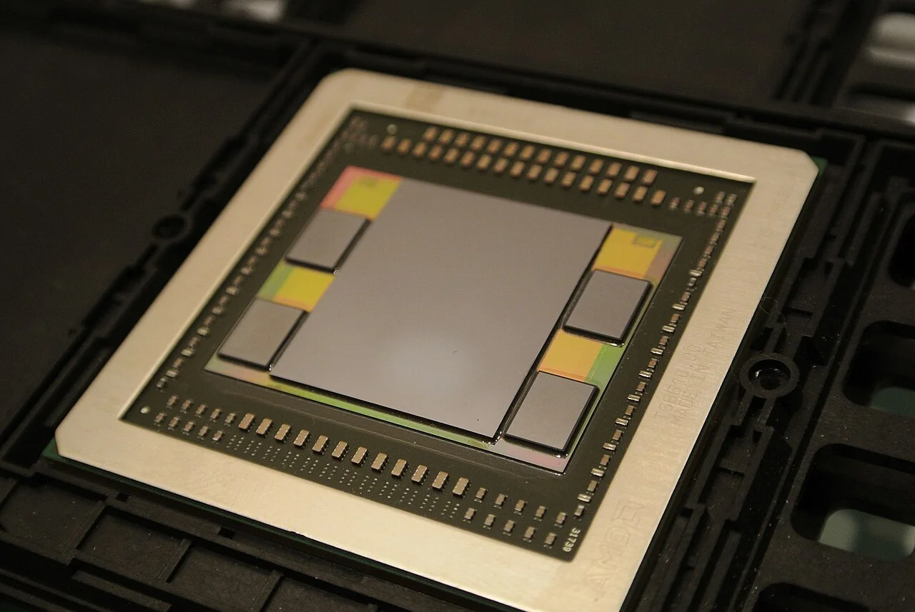
The HBM used in today’s high-end AI servers sits in a 2.5D package: the GPU or AI accelerator and the memory sit side by side on a silicon interposer. Stacking DRAM dies vertically raised bandwidth, but data between the accelerator and HBM still travels horizontally through the interposer’s wiring.
As large language models and agentic AI handle more data at once, that horizontal link carries more strain. Longer wires add delay and power loss, and a bigger package makes power delivery and heat management harder.
How Samsung zHBM differs from HBM
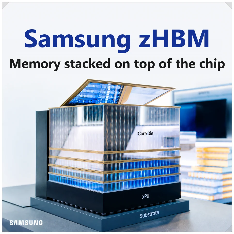
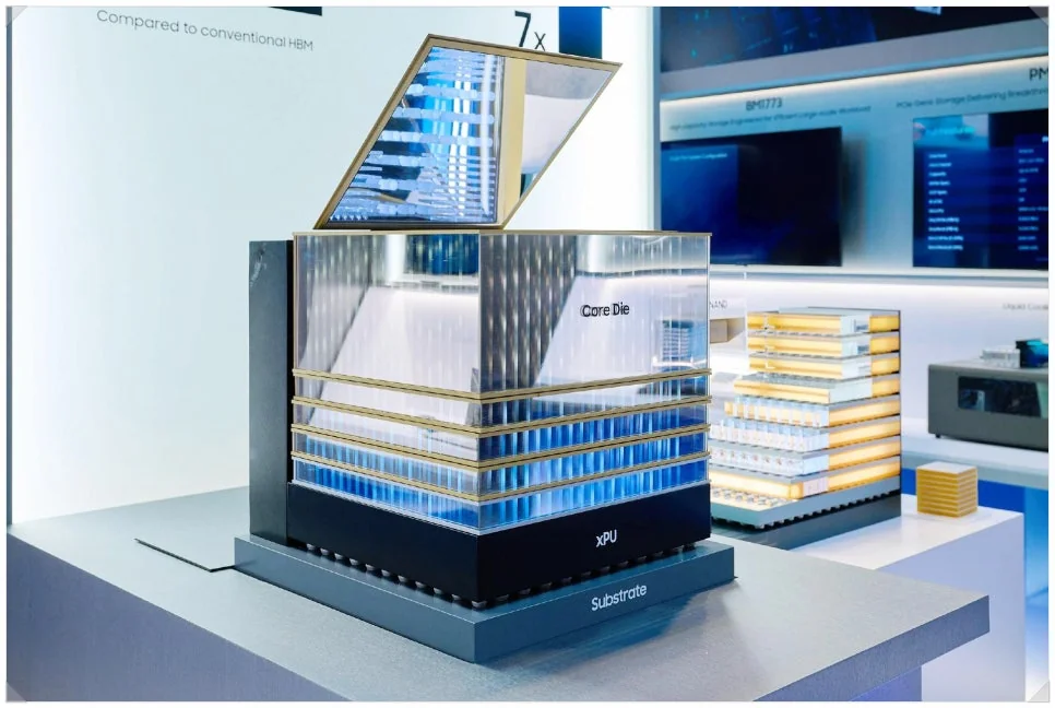
As the name suggests, zHBM uses the Z axis, or height. It stacks DRAM directly on top of the xPU accelerator and joins them into one 3D structure. The physical distance between accelerator and memory shrinks from millimeters to micrometers, which cuts the time and power data movement takes.
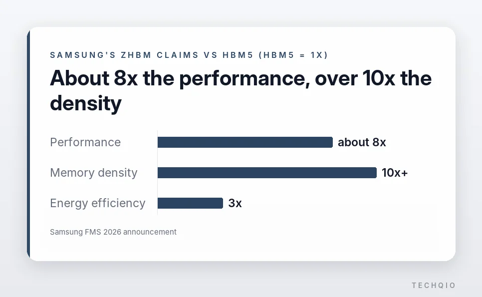
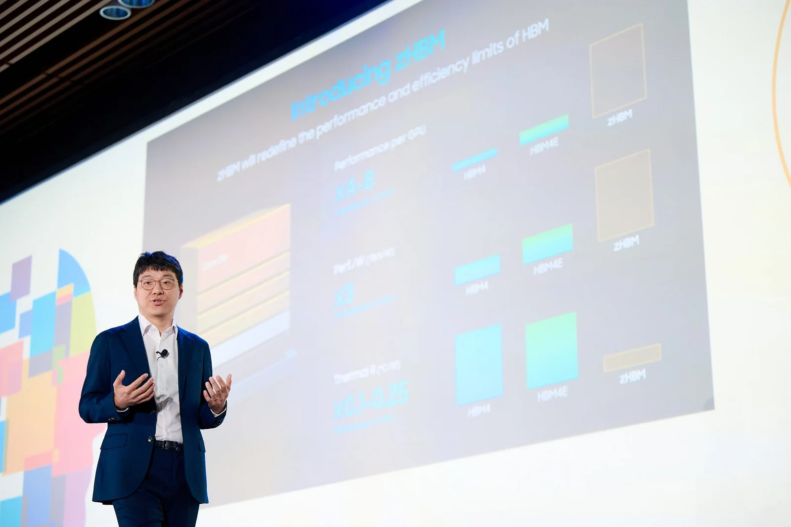
According to Samsung’s FMS 2026 announcement, zHBM delivers about eight times the performance of HBM5, the next-generation standard, and more than 10 times the memory density of HBM5.
Energy efficiency improves threefold, and thermal resistance drops by more than half. Samsung’s keynote slide framed the comparison against HBM4 and HBM4E instead: 4 to 8 times the performance per GPU, three times the performance per watt and 0.1 to 0.25 times the thermal resistance.
This goes a step beyond adding more HBM layers to raise bandwidth. It changes how the accelerator and memory are connected in the first place.
| Spec | Today’s 2.5D HBM | Next-gen 3D zHBM |
|---|---|---|
| Chip layout | Side by side on a silicon interposer | Stacked vertically on the xPU |
| Connection | Micro bumps and interposer wiring | Bumpless Cu-Cu hybrid bonding |
| Performance | Bandwidth rises each generation | About 8x HBM5 performance, 3x energy efficiency |
| Custom design | Limited, mostly in the base die | Customer IP built into the interlayer |
The interlayer opens up custom designs
The part of zHBM to watch is the custom interlayer between memory and accelerator. The base die in today’s HBM mainly handles signal transfer and I/O control. In zHBM, customers can put their own IP and control circuits into the interlayer.
Typical examples are in-memory computing that runs part of the work inside memory, or cache-control logic tuned to a specific AI accelerator. Because data flow can be designed around a customer’s chip and workload, it helps fine-tune AI inference latency and power use.
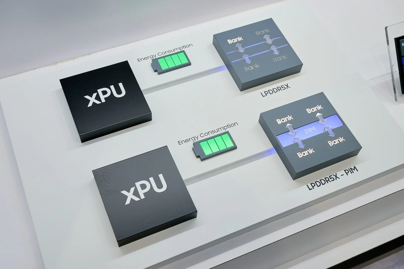
This shift changes the memory maker’s role too. In the past the job was to supply DRAM built to JEDEC standards. Co-design, where fabless chip designers and memory makers settle the chip structure together from the earliest architecture stage, is likely to matter more.
Samsung’s one-stop pitch
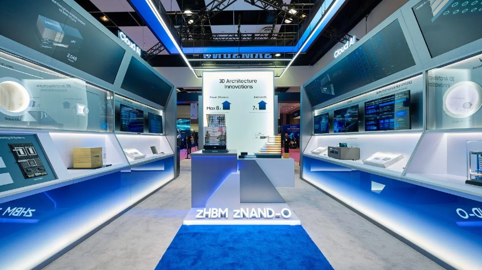
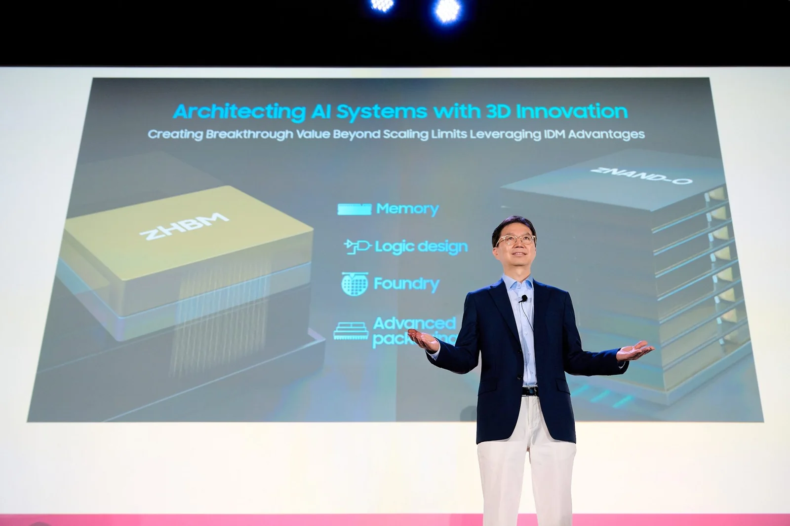
At the FMS 2026 keynote, Kyungryun Kim, vice president of Samsung’s DRAM design team, and Jin-Yub Lee, executive vice president and head of flash product and technology, presented Samsung’s 3D memory vision under the message “Samsung is back.” The products on display were mockups, not production parts, but the industry’s interest in how zHBM would be built and brought to market was clear.
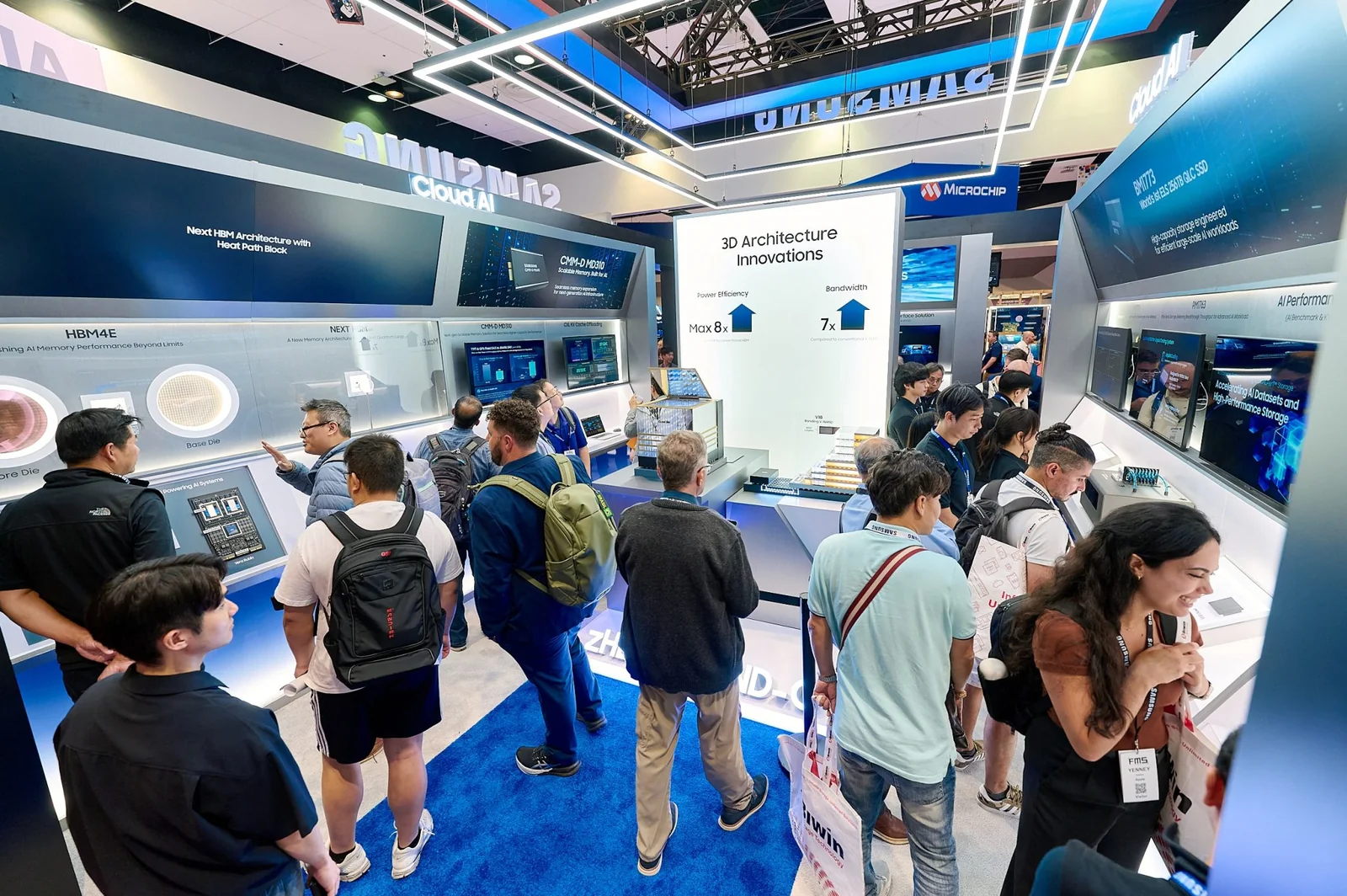
zHBM is hard to build with memory design alone. It needs high-performance DRAM, advanced foundry processes, wafer bonding and 3D packaging working together. Samsung runs memory, foundry and packaging businesses, and it pitches its ability to tune the interface between logic chip and DRAM in-house as an advantage.
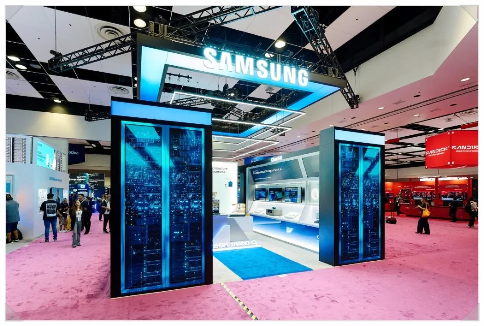
Putting a customer’s circuits into the interlayer takes close cooperation between the memory, foundry and packaging teams. Coordinating every step in one development system can shorten development time and improve product quality.
zHBM will not replace 2.5D HBM right away. Before mass production and wider adoption, Samsung has to solve heat, bonding yield and the cost of moving customers’ ecosystems.
Three hurdles before zHBM ships
Three problems stand between the mockup and a product: heat, bonding yield and the cost of switching from today’s packaging.
1. Thermal interference
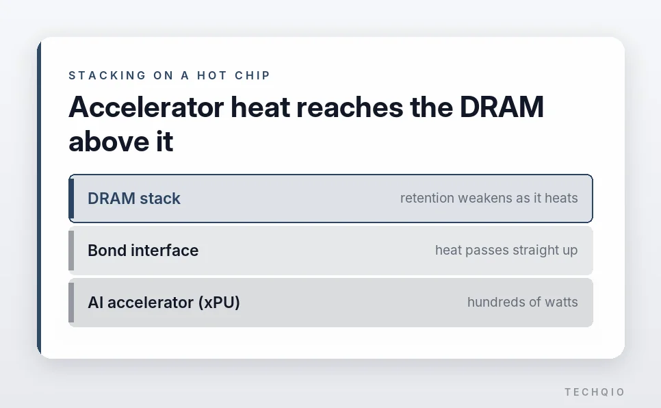
Put DRAM directly on an AI accelerator that draws hundreds of watts, and the accelerator’s heat flows straight into the memory. As DRAM gets hotter, charge leakage rises and data retention can suffer, so designers need to weigh heat-blocking structures, liquid cooling and heat-spreading materials together.
2. Wafer-to-wafer bonding yield
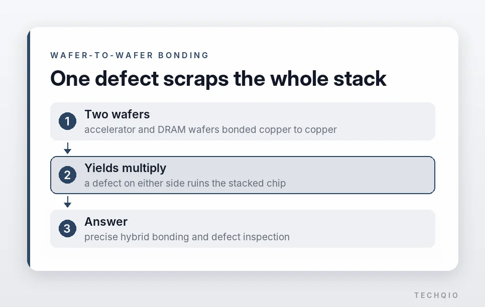
When an accelerator wafer and a DRAM wafer are bonded copper to copper without bumps, both wafers’ yields carry into the final product. A defect on either side makes the whole stacked chip unusable, so precise hybrid bonding and defect inspection are essential.
3. Switching costs for the ecosystem
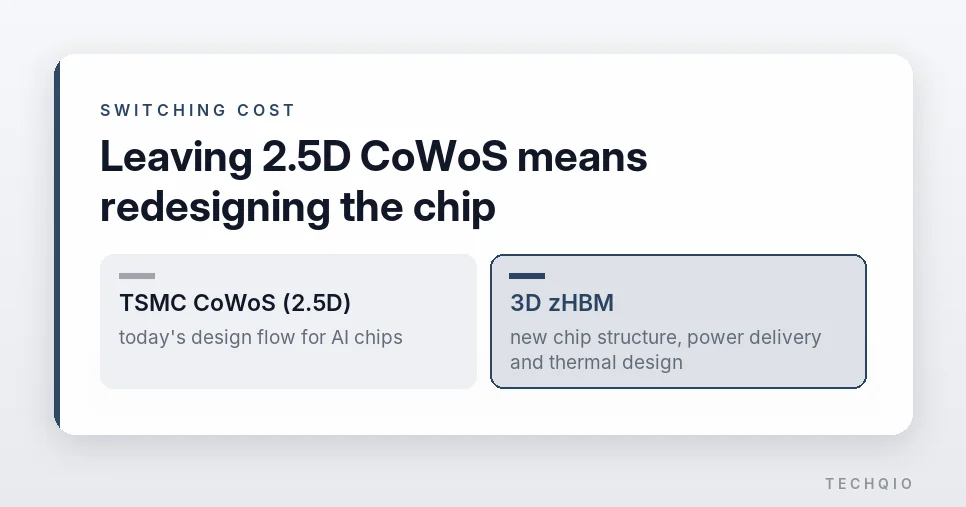
Major AI chip companies already build their products around TSMC’s 2.5D CoWoS process and design flow. Adopting zHBM means rethinking chip structure, power delivery and thermal design, so it has to show performance and efficiency gains clear enough to justify the upfront development cost.
Samsung and SK hynix take different routes
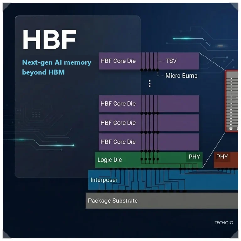
At FMS 2026, the two Korean memory makers showed different answers. Samsung focused on a dense structure that joins accelerator and memory vertically with zHBM. SK hynix stressed capacity expansion built around HBF, its high-bandwidth flash, and CXL-based CMM memory; it and Sandisk released the first HBF specification through the Open Compute Project the same week.
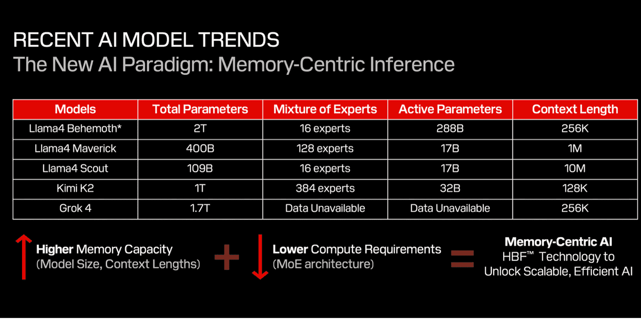
Samsung’s approach shortens the distance between compute and memory to raise bandwidth and power efficiency. SK hynix’s approach leans toward pooling, where several devices share memory resources, and NAND flash’s capacity advantage, to enlarge the total memory space of an AI system.
The two are different responses to the same infrastructure bottleneck:
- When data transfer speed and power efficiency around the AI accelerator matter most, vertical designs like zHBM fit.
- When large-scale storage and memory expansion matter most, HBF and CXL-based technologies fit.
What zHBM signals for AI memory
If Samsung zHBM reaches production, it could improve the power and space efficiency of AI data centers. More memory in the same area and shorter data paths could also lower server and cooling costs, and in the long run the approach could raise on-device AI performance in phones and PCs.
The next milestones are a production schedule and a first customer, along with proof that heat and bonding yield are under control. Until then, zHBM is less an HBM replacement than a preview of where AI chip packaging is headed: compute and memory fused into one 3D structure.