CXMT 4F² DRAM: Can China’s New Memory Tech Really Threaten Samsung and SK Hynix?
Key takeaways
- CXMT plans a 4F² server DDR5 RDIMM by end of 2026, about a third smaller per cell
- Without EUV tools, CXMT relies on DUV and quadruple patterning; yield and specs are undisclosed
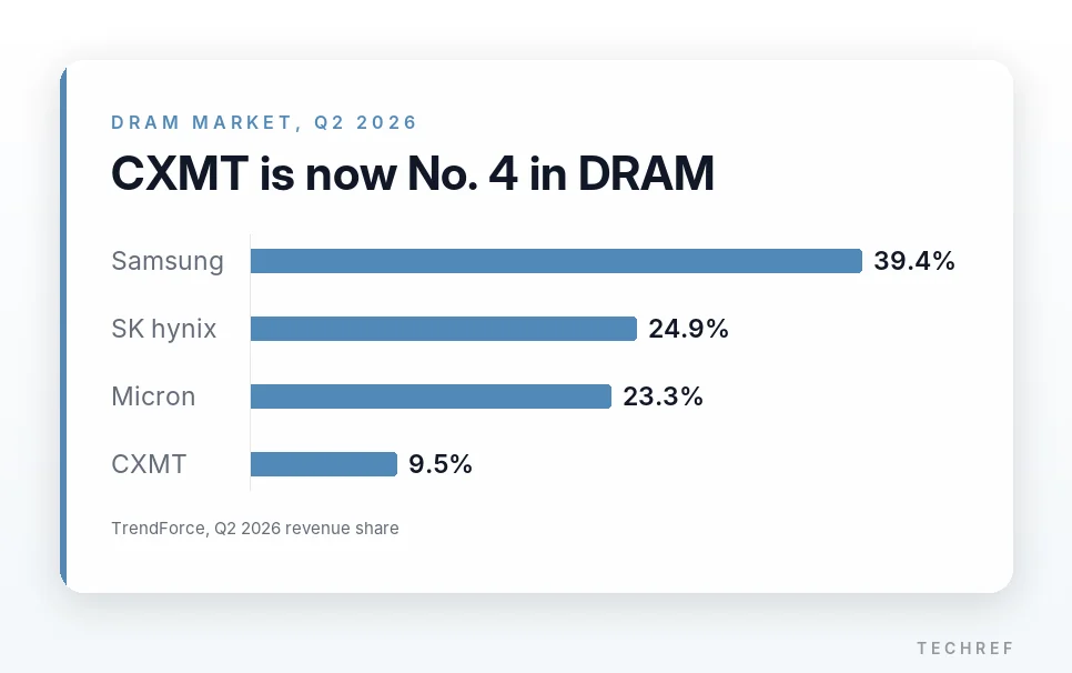
- CXMT reached 9.5% DRAM share in Q2 2026, behind Samsung, SK hynix and Micron
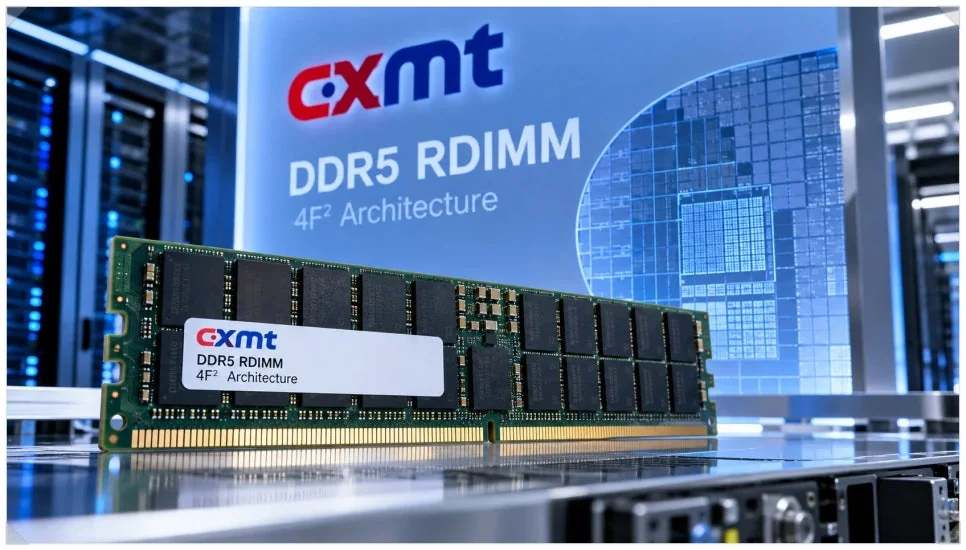
China’s CXMT has unveiled next-generation DRAM technology, and Samsung and SK hynix are feeling the pressure. At a conference in Shanghai in October, CXMT said it would launch CXMT 4F² DRAM in server DDR5 RDIMM modules by the end of the year. Afterward, Samsung shares fell 7.39% and SK hynix dropped 10.09%.
4F² shrinks the area of each memory cell, but CXMT still has plenty of hurdles to clear before mass production.
4F²: a smaller DRAM cell
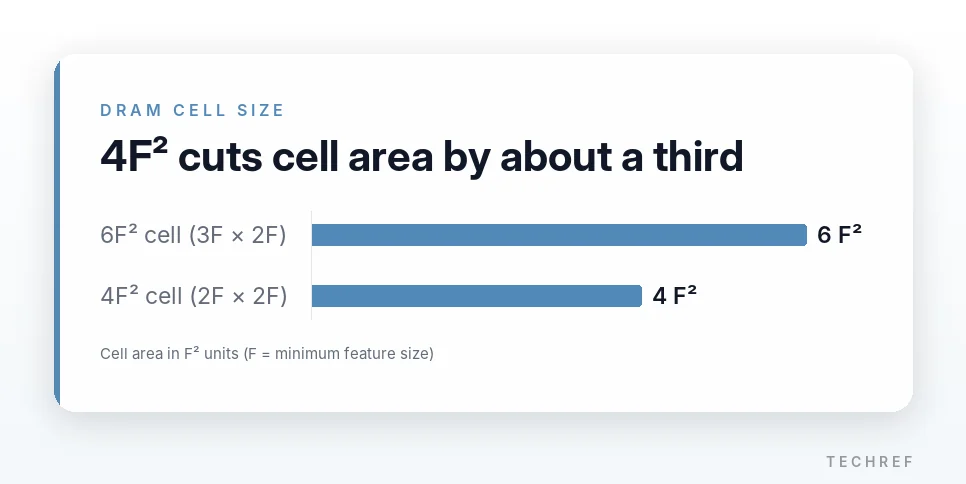
Today’s DRAM stores data with one transistor and one capacitor per cell. The most common cell layout is 6F². Here, F (feature size) is the minimum line width used as the baseline when designing chip circuits.
A 6F² cell occupies a rectangle 3F wide and 2F tall. A 4F² cell is a 2F-by-2F square. At the same line width, that cuts the area of each cell by about 33% in theory.
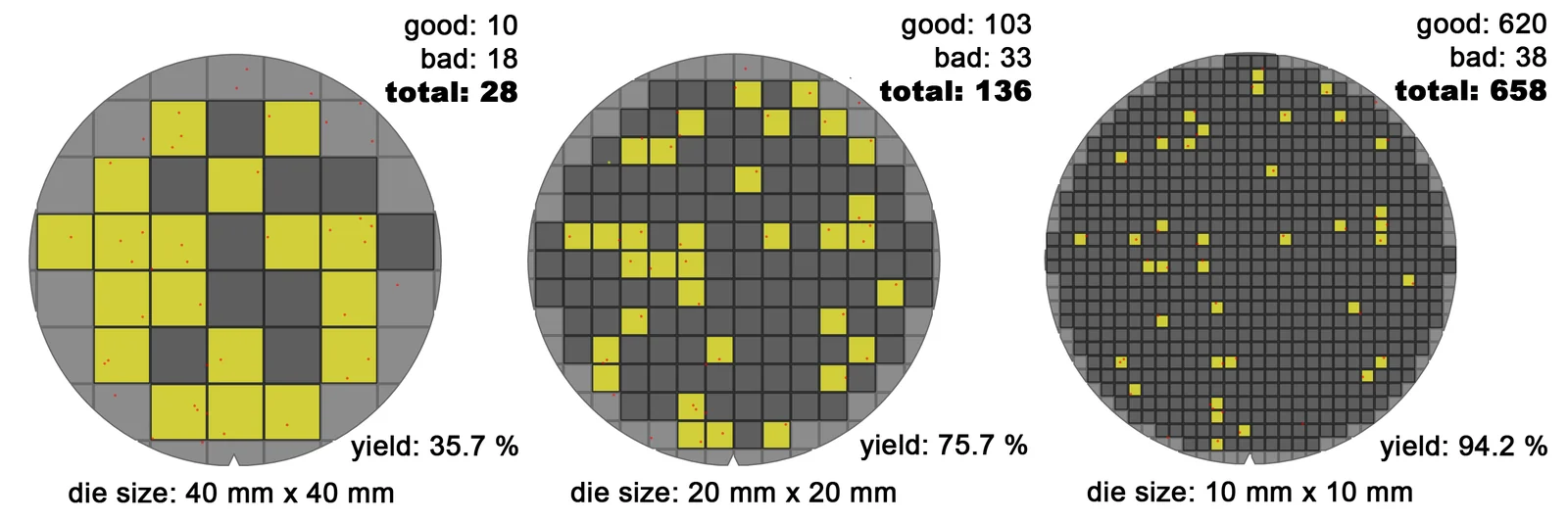
Smaller cells mean more memory fits on a wafer of the same size. Depending on design and process conditions, chip density can rise 30 to 50%. Actual output, though, depends on the area of the peripheral circuits and on yield.
Getting there also requires a new transistor structure. The key is the vertical channel transistor (VCT), which stands the transistor upright instead of using a horizontal channel.
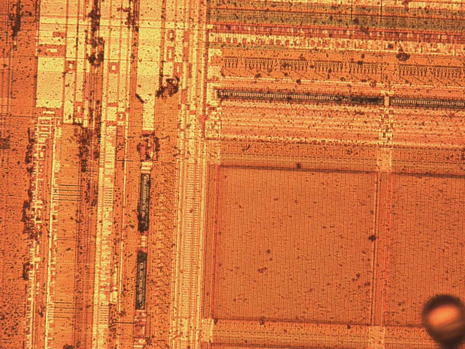
As DRAM line widths shrink to around 10 nanometers, short-channel effects get worse: current leaks in directions it shouldn’t. When stored charge drains quickly, it gets harder to hold data reliably.
To reduce this, CXMT says it uses a Vertical Surrounded Gate (VSG), in which the gate wraps around a vertical channel. Standing the transistor up saves area and also suppresses leakage current.
| Current 6F² | Next-gen 4F² | |
|---|---|---|
| Cell layout | 3F × 2F | 2F × 2F |
| Cell area | Baseline (100%) | About 33% smaller in theory |
| Transistor | Mainly horizontal channel | Vertical channel (VCT, VSG) |
| Chip density | Baseline | About 30–50% higher possible |
| Main challenge | Optimizing existing processes | Redesigning wiring and bonding steps |
CXMT 4F² DRAM: can it actually be mass-produced?
The 4F² structure helps pack in more memory, but it’s hard to bring into real chip production. Lithography, the step that prints tiny circuits onto the wafer, is expected to be especially difficult.
Because of US-led chip export controls, China can’t easily get ASML’s advanced extreme ultraviolet (EUV) lithography tools from the Netherlands. CXMT has to use older deep ultraviolet (ArF immersion DUV) tools and add extra process steps.
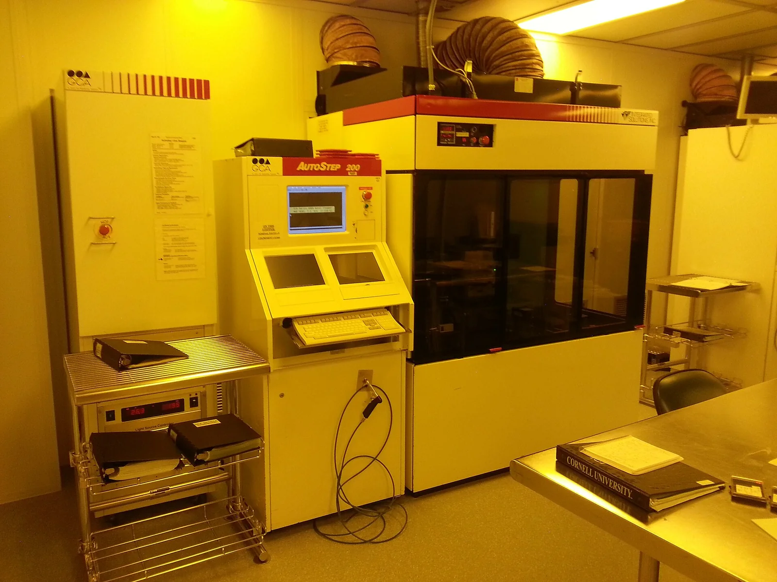
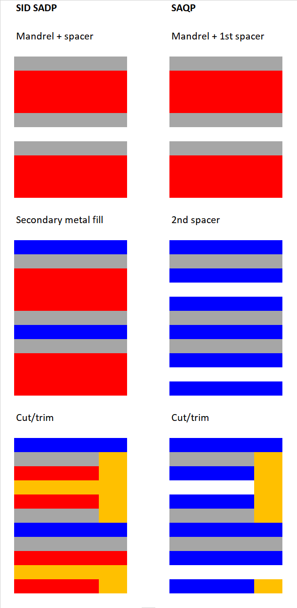
The main technique is self-aligned quadruple patterning (SAQP).
It forms circuits too fine to print in one pass over several steps. The more complex the process, the more likely alignment errors and defects become, and manufacturing costs can rise too.
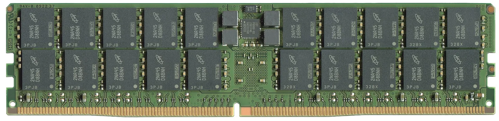
It also matters that the product CXMT previewed is a server DDR5 RDIMM, a registered memory module for servers.
Data center servers must run reliably around the clock, and even small memory errors can disrupt operations. That means error correction (ECC), long-term reliability testing and compatibility with major CPU platforms all need thorough validation.
In September, CXMT announced mass production of LPDDR5X on its fifth-generation G5 platform, with an 11.95-nanometer half-pitch. But making mobile memory is a different problem from reliably supplying server products built on a new 4F² structure.
CXMT hasn’t disclosed speed, power consumption, capacity or yield. Without those figures, it’s unclear whether this year’s launch means real volume supply or only early engineering samples.
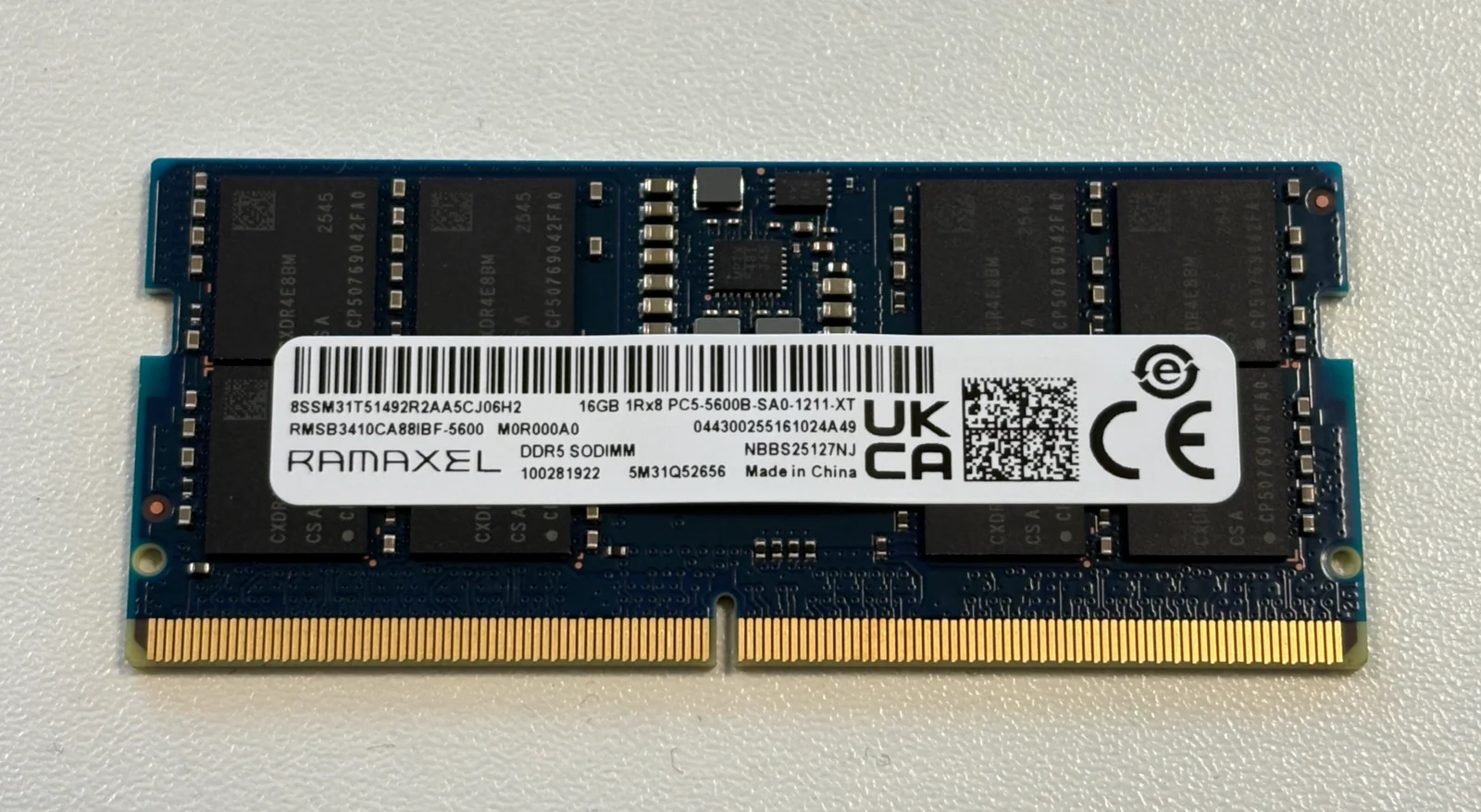
How Samsung and SK hynix are approaching next-gen DRAM
Samsung and SK hynix are also researching 4F² as their next-generation DRAM technology.
Their process targets and development direction differ from CXMT’s, though.
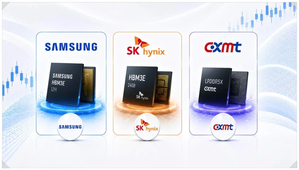
Samsung plans to apply vertical channel transistors at its D0a node, an ultra-fine process below 10 nanometers.
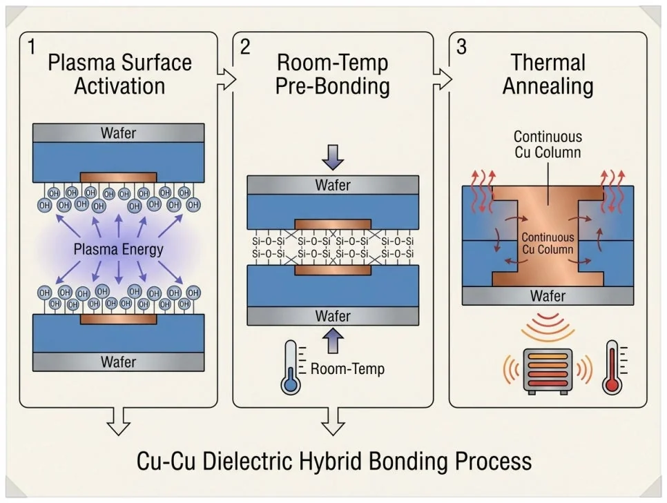
It’s also looking at wafer-to-wafer (W2W) hybrid bonding, which builds the memory cells and the peripheral control circuits (Peri) on separate wafers and then bonds them vertically. The goal is to shrink cell area while laying out circuits efficiently, raising the density of the whole chip.
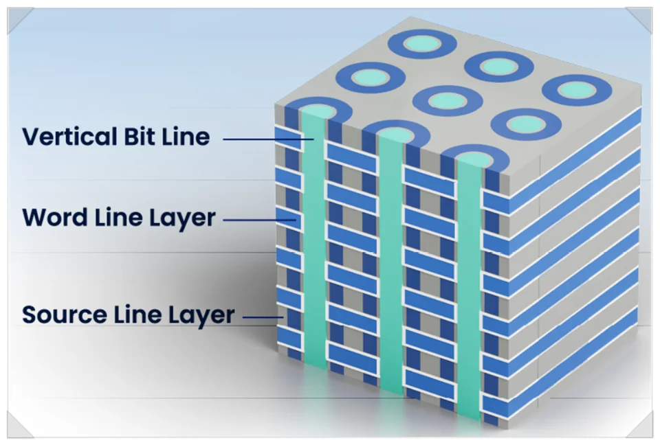
SK hynix presented a 4F² platform based on a vertical gate (VG) at the IEEE VLSI Symposium. It uses PUC, which places the peripheral circuits under the memory cells, and is researching a path toward 3D DRAM in the long run.
Korean chipmakers are advancing sub-10-nanometer processes and advanced packaging together. Some expect mass production around 2028, but the actual schedule will depend on technical maturity and market conditions.
CXMT, by contrast, chose to apply 4F² first on a 15-nanometer-class process, which has more manufacturing headroom. That lowers process difficulty and could bring its product out about two years earlier.
The same 4F² label can mean very different processes and manufacturing difficulty. That’s why launch timing alone doesn’t show that Samsung and SK hynix have fallen behind.
A 9.5% share: China’s DRAM momentum
According to TrendForce, CXMT held a 9.5% share of the global DRAM market in Q2 2026, up from 7.6% the previous quarter, and its revenue roughly doubled.
In the same quarter, Samsung had 39.4%, SK hynix 24.9% and Micron 23.3%. CXMT has grown into the world’s No. 4, but the top three still hold most of the market.
Rising prices for commodity DRAM also lifted CXMT’s share. In Q2, growing AI infrastructure spending and tight supply pushed memory prices sharply higher. With a product mix weighted toward commodity chips, CXMT benefited from that price-driven revenue growth.
SK hynix sells much of its high-bandwidth memory (HBM) under long-term contracts, so price swings flow into its revenue differently. TrendForce notes SK hynix’s price growth was limited because HBM made up the largest share of its shipments. Revenue growth alone isn’t a fair way to compare the two companies’ technology.
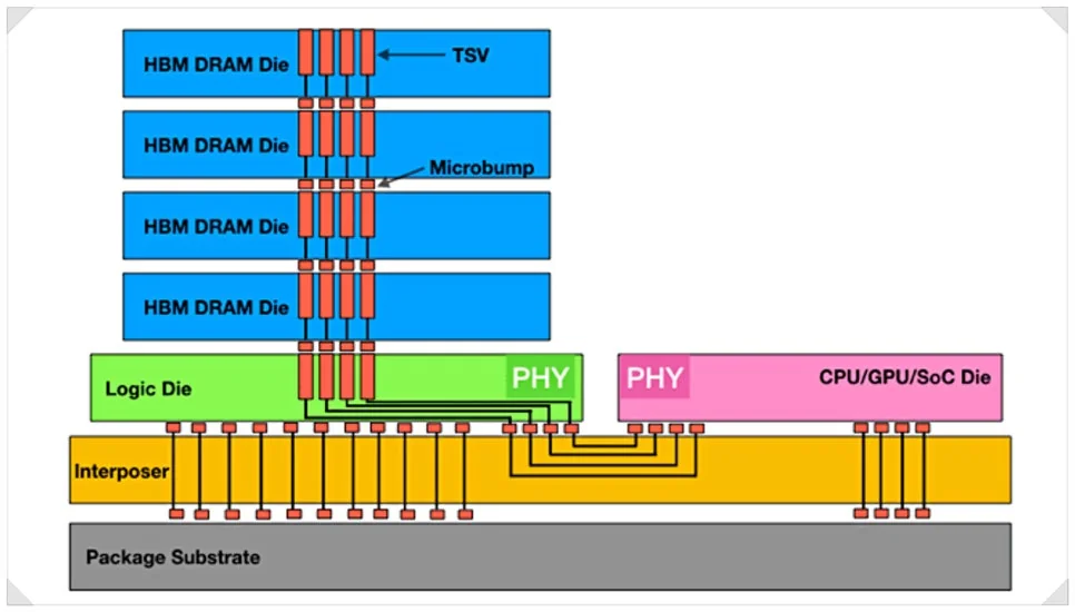
In HBM, most assessments still put Korean companies in the lead.
Some analyses put China’s technology gap at three years or more. That varies by product and by how you measure it, though, so it doesn’t apply equally to every type of memory.
CXMT’s capacity expansion is the next thing to watch.
Its wafer capacity is estimated at around 300,000 wafers per month. Forecasts call for 420,000 a month in 2027 and, once new fabs in Hefei and Shanghai are finished, as many as 600,000 a month over the long term.
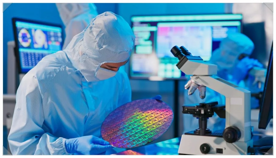
If CXMT also nails 4F² production efficiency, its supply of commodity DDR5 could grow substantially. If it expands supply mainly to data centers inside China, that could also affect global memory prices.
Of course, more fab capacity doesn’t immediately mean more shipments. CXMT still has to raise yields, cut manufacturing costs and win customers. But if the memory market turns down, China’s added supply could intensify price pressure.
Bottom line: what to watch in China’s DRAM push
The CXMT 4F² DRAM announcement shows China is accelerating next-generation DRAM development. Still, building a new structure is one thing and mass-producing it reliably is another. Real performance, yield and adoption by server makers will show where the technology actually stands.
Samsung and SK hynix need to stay competitive not only in HBM3E and HBM4 but also in next-generation 4F² processes. CXMT’s capacity growth after 2027 could also affect commodity DRAM prices, which matters for Micron and memory buyers in the US too.