What Is HBF? High Bandwidth Flash vs HBM, the Next AI Memory
Key takeaways
- HBF stacks NAND flash like HBM stacks DRAM, trading some speed for far more capacity.
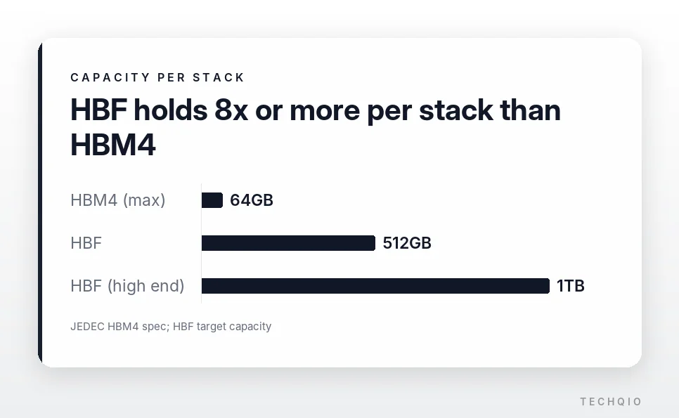
- One HBF stack targets 512GB to 1TB, versus a 64GB maximum under the HBM4 spec.
- Sandisk and SK hynix published the first HBF specification on Aug. 3, 2026.
High Bandwidth Flash (HBF) stacks NAND flash the way HBM stacks DRAM, and chipmakers see it as a way past HBM’s structural limits. HBM, or high-bandwidth memory, comes up in almost every AI story: demand has grown so fast that NVIDIA GPUs sell out, and the HBM inside them has become one of the most valuable parts in the chip industry.
One HBF stack targets 512GB to 1TB, eight to 16 times the 64GB an HBM4 stack can hold, and Sandisk and SK hynix published its first specification in August 2026. That capacity is what could make large AI models cheaper to run.
What is High Bandwidth Flash?
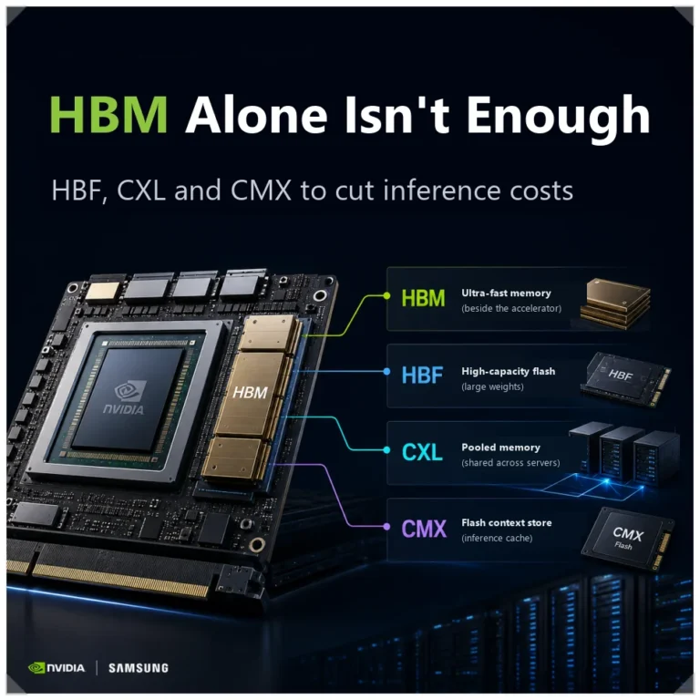
When a large language model like ChatGPT answers slowly or costs a lot to run, memory capacity is often part of the reason. HBM, the main memory in today’s AI accelerators, is extremely fast, but it is expensive and holds only so much.
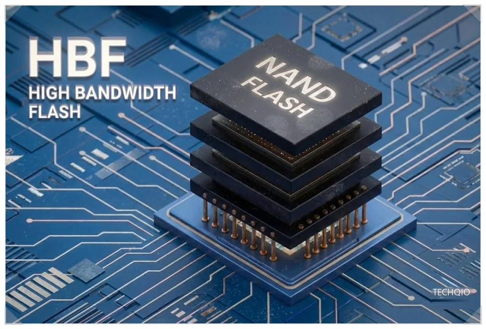
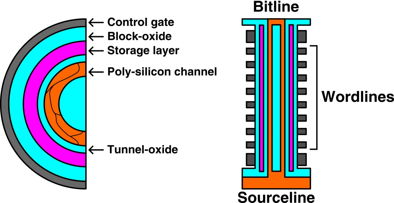
High Bandwidth Flash is the answer to that problem. Put simply, it piles NAND flash, the memory used for storage, into a tall vertical stack, which sharply raises speed while storing far more data than HBM. Sandisk says in its Memory-Centric AI blog post that it invented HBF to close the gap between AI models’ memory demands and DRAM’s slow progress, a gap known as the memory wall.
HBF vs HBM: what is the difference?
Picture a study. HBM is a small shelf right next to the desk, and HBF is a large bookcase filling a whole wall. You can grab a book from the desk shelf instantly, but it holds only a few. The wall bookcase takes a moment longer to reach, yet it stores far more knowledge than the shelf ever could.

The same split shows up in how AI works. Training reads and writes data constantly, so ultra-fast HBM is essential. Inference, where a trained model generates answers, depends on laying out huge amounts of data at once and referring to it, so high-capacity HBF is seen as the more efficient fit.
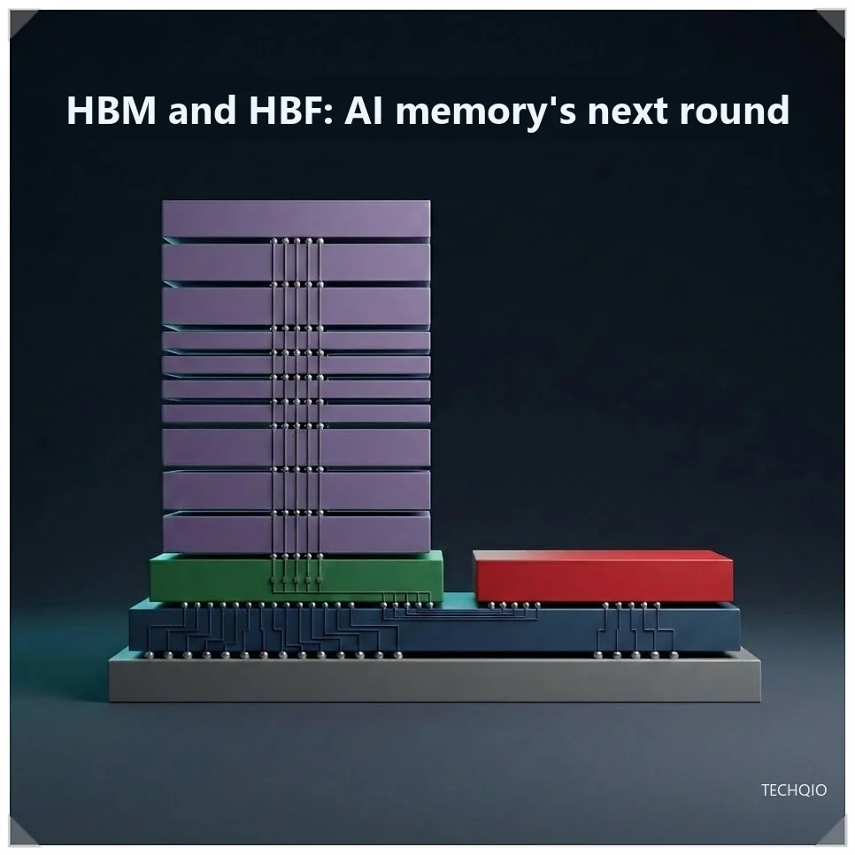
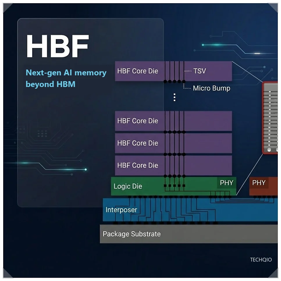
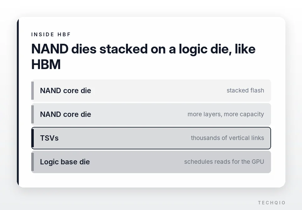
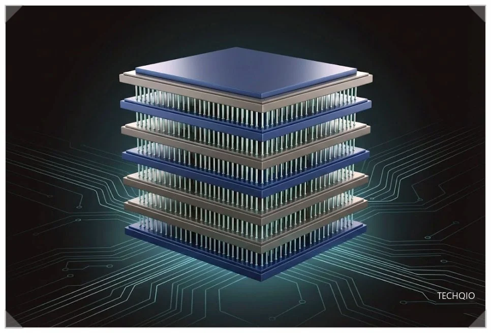
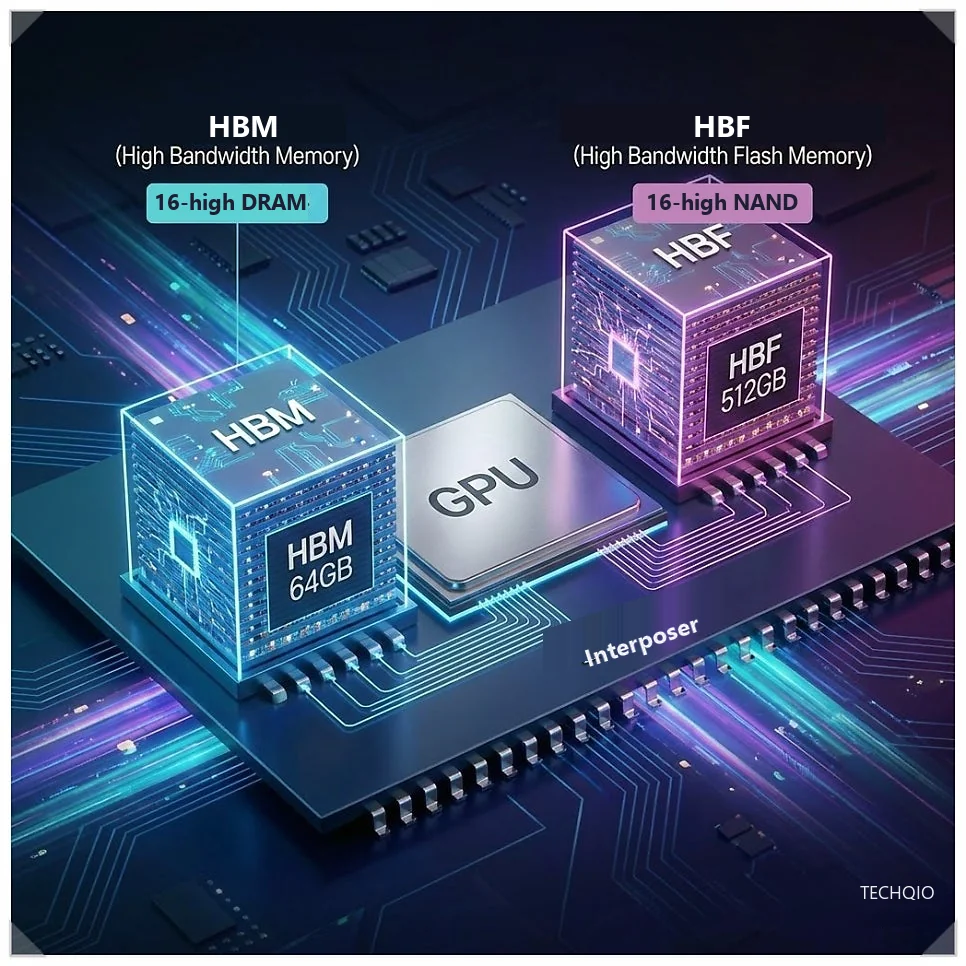
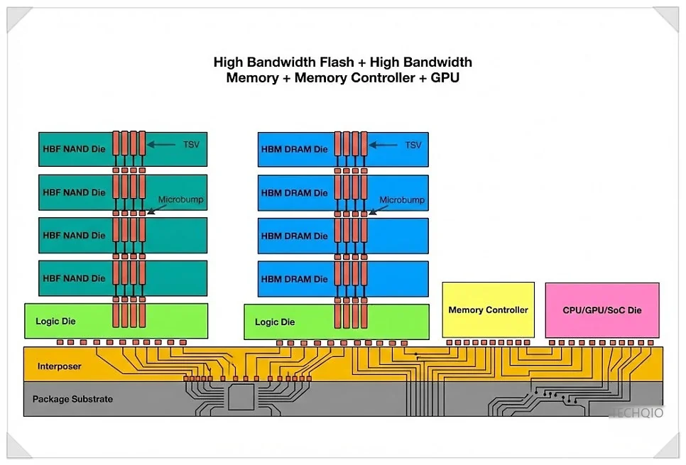
Structurally, the two are close cousins. Both use TSVs (through-silicon vias) to connect stacked chips vertically and sit beside the processor on a silicon interposer. The decisive difference is what goes inside: DRAM or NAND flash.
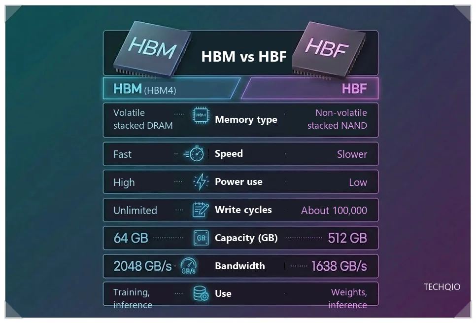
Here is how the two compare side by side.
| Spec | HBM (High Bandwidth Memory) | HBF (High Bandwidth Flash) |
|---|---|---|
| Core material | DRAM (loses data without power) | NAND flash (keeps data without power) |
| Capacity per stack | Up to 64GB under the HBM4 spec | 512GB to 1TB or more |
| Transfer speed | Very high (up to 2 TB/s per HBM4 stack) | High (about 1.6 TB/s target) |
| Main role | AI training and real-time compute | AI inference and large data caching |
| Cost | Very expensive | Relatively cheaper |
HBF’s biggest strength is capacity. The JEDEC HBM4 standard tops out at 64GB per stack with 16 layers of 32Gb dies, while a single HBF stack can hold 512GB and up to 1TB. HBF targets bandwidth of about 1.638 TB/s, tens of times faster than the SSDs most people use, to feed data to the GPU.
The trade-off is endurance. NAND cells wear out after about 100,000 write cycles, while DRAM has no such limit, which is one reason HBF suits read-heavy inference rather than training.
How does HBF get 1.6 TB/s out of slow NAND?
NAND flash has a reputation for being slow, so how does HBF reach this kind of bandwidth? The answer is parallelism. Conventional NAND sends data through a fairly narrow path, one piece after another. HBF stacks many NAND chips vertically and pushes data through thousands of TSVs at once.
Sandisk and SK hynix both point to the same key part: the logic base die. It works like the building manager of the NAND stack, organizing data from slow-reading NAND in advance and managing bottlenecks so the GPU is not left waiting.
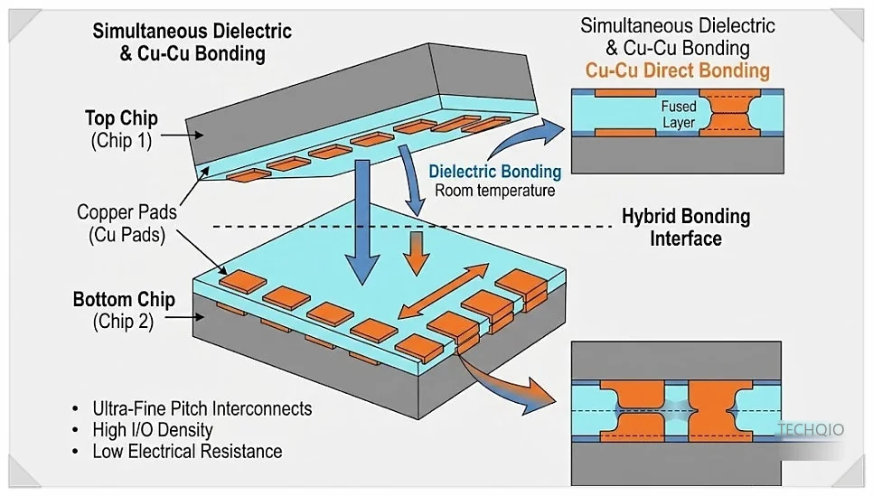
Add hybrid bonding, which connects chips directly to each other, and the path data travels gets even shorter.
Samsung, SK hynix and Sandisk take different paths
The companies around HBF are moving quickly, and the most aggressive is SK hynix, today’s HBM leader. It announced an AI-focused NAND lineup called AIN (AI-NAND), and the bandwidth-focused AIN B line in its NAND strategy is the HBF product, built from stacked NAND dies.
The partnership with Sandisk, one of the pioneers of NAND, stands out. The two companies laid out a fairly specific roadmap of prototypes in the first half of 2026, then mass production and supply to customers such as NVIDIA in 2027. Their standards work has moved on schedule: Sandisk and SK hynix released the first HBF technical specification through the Open Compute Project on Aug. 3, 2026, six months after they started the work, and Google and Tenstorrent joined the consortium.
Samsung is taking a different approach. It already has its own hybrid memory technology, such as CMM-H (CXL Memory Module-Hybrid), so rather than going all in on HBF, it chose to watch the market and join the related consortium.
Samsung’s strength is turnkey production that spans memory, foundry and packaging. It is counting on V-NAND with 400 or more layers, targeted for 2026, to take the lead quickly once the market opens in earnest.
Will HBF replace HBM?
Once HBF is commercialized, the first change people will feel is cheaper and faster AI services. Running a large model today means tying together several very expensive GPUs. With HBF, fewer GPUs could handle massive data efficiently, which lowers operating costs for companies and means faster, cheaper AI services for users.
High Bandwidth Flash will not fully replace HBM. More likely, the two will coexist, much as the human brain splits short-term and long-term memory:
- HBM where ultra-fast compute is needed
- HBF where vast knowledge has to be stored
The first HBF specification is now public. The next proof points are shipping HBF parts and an AI accelerator that uses them alongside HBM; until both arrive, HBF is a design target rather than a product you can buy.