AI Inference Memory: How HBF, CXL and CMX Cut Costs
Key takeaways
- Inference, not training, now drives AI memory demand, and the KV cache is what fills HBM.
- HBF adds stacked flash next to HBM. Its first OCP spec came out Aug. 3, 2026.
- CXL lets one machine borrow DRAM from another, and NVIDIA’s CMX puts a G3.5 layer of Ethernet-attached storage under HBM.
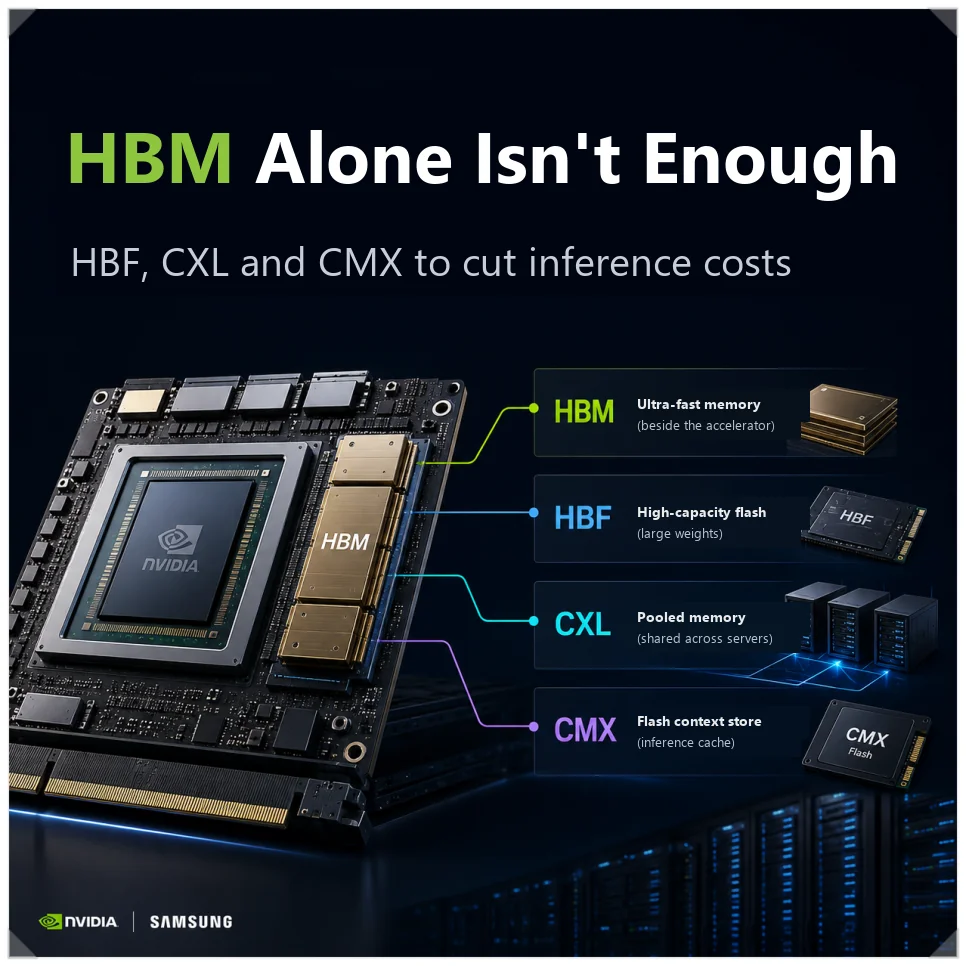
High-bandwidth memory made the AI training boom possible by feeding GPUs data fast enough to keep them busy. Now that the money is moving from training to serving models, AI inference memory has a different job. It has to hold huge amounts of context cheaply as well as move it quickly. That is the problem HBF, CXL and NVIDIA’s CMX are built to solve.
Inference servers answer requests from many users at once and keep long conversations alive. That takes capacity and cost efficiency as much as speed. HBM alone cannot supply all three. So each of the three technologies adds a cheaper place to keep data that HBM cannot hold.
Why inference now costs more than training
For years, the AI race was about training, which means feeding huge datasets into ever-larger models. The weight is shifting to inference, where a finished model answers user questions in real time. In 2026, inference already accounts for more than 65% of global AI compute. It is also expected to drive more than 70% of data center AI demand by around 2030.
The two workloads also do different math. Training runs a forward pass and then backpropagation, which adjusts the weights based on the error, for roughly 6 FLOPs per parameter per token. Inference keeps the trained weights fixed and runs only the forward pass, which cuts the work to about 2 FLOPs per parameter per token.
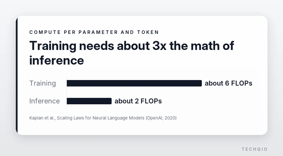
Per request, inference looks cheap. But training cost is paid once, while inference cost repeats every time someone uses the service. GPU time and memory use climb with every user and every token. Once cumulative inference tokens pass about three times the data used to train the model, running costs can exceed the original training bill.
| Aspect | AI training | AI inference |
|---|---|---|
| How it computes | Optimizes weights with backpropagation | Generates tokens with fixed weights |
| Compute per parameter and token | About 6 FLOPs | About 2 FLOPs |
| Main bottleneck | Communication between nodes and the network | Memory capacity, bandwidth and access latency |
| Cost profile | Large up-front investment during development | Operating cost that repeats with usage |
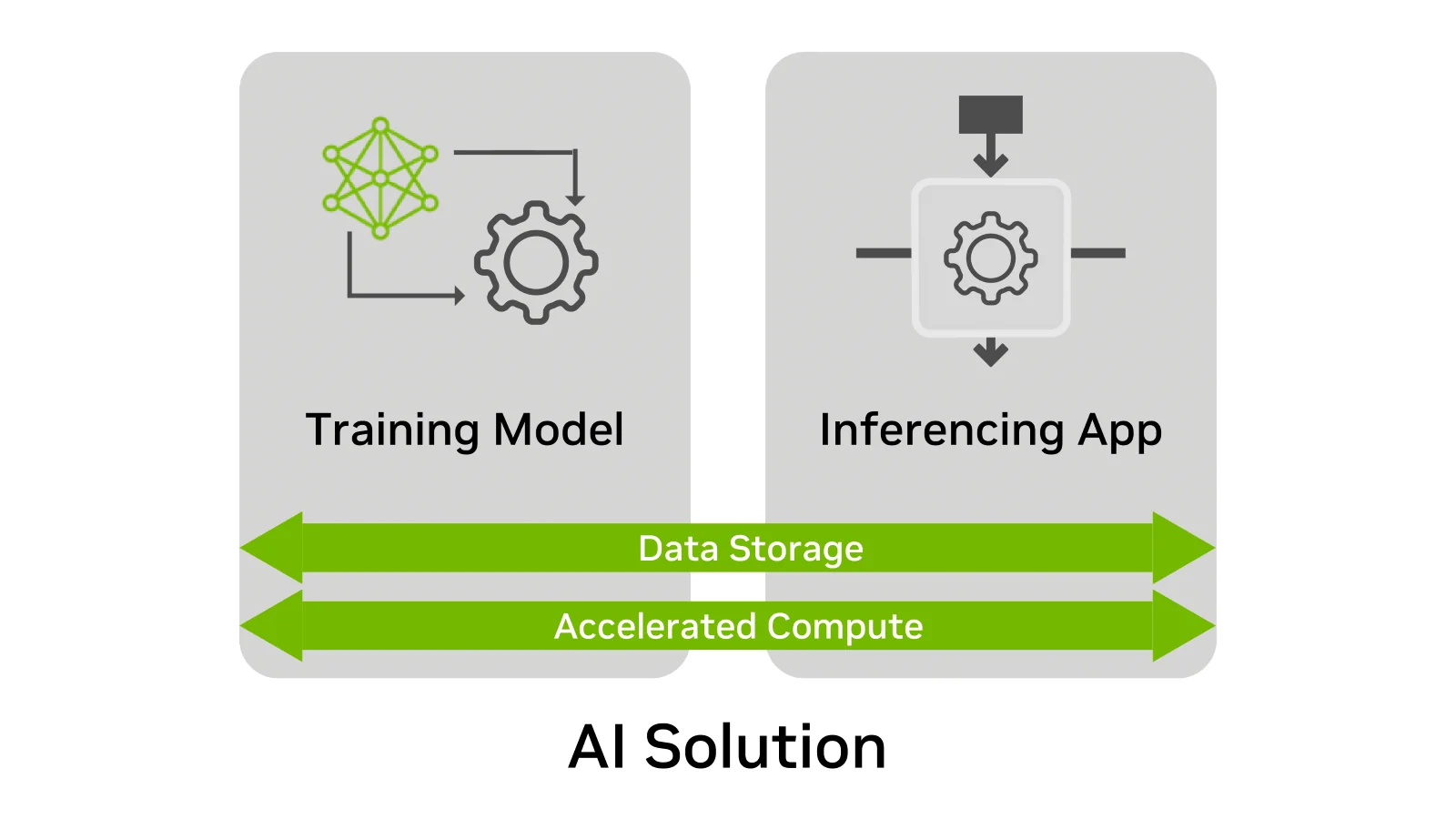
An inference server has to handle many requests at the same time. Beyond GPU power, it needs enough memory for the model weights and for each user’s context. That is why memory prices and supply feed straight into the cost of running an AI service. The large AI infrastructure budgets that Microsoft, Google, Amazon and Oracle have planned for 2026 reflect the same shift.
Why the KV cache dominates AI inference memory
Large language model inference runs in two phases. Prefill reads the whole prompt and context at once. Because many tokens are processed in parallel, GPU compute matters most. Decode then generates the answer one token at a time. Since each new token has to look back at everything before it, memory bandwidth and latency matter more than raw compute.
The data that eats that memory is the KV (key-value) cache. Instead of recomputing the earlier context for every token, the model stores intermediate results and reloads them to continue the conversation.
Meta’s Llama 3 paper lists 32 layers and 8 key-value heads (grouped-query attention) for the 8B model, with 128 dimensions per head.
At half precision (FP16), the keys and values for one token take 32 × 8 × 128 × 2 × 2 bytes, or about 128 KB in the standard configuration (other settings change the figure). A one-million-token job can therefore need about 125 GB of fast memory per GPU on top of the model itself.
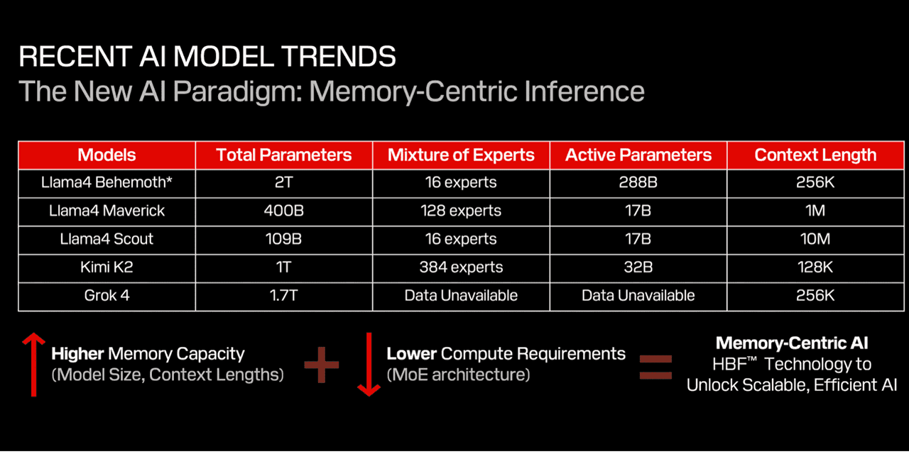
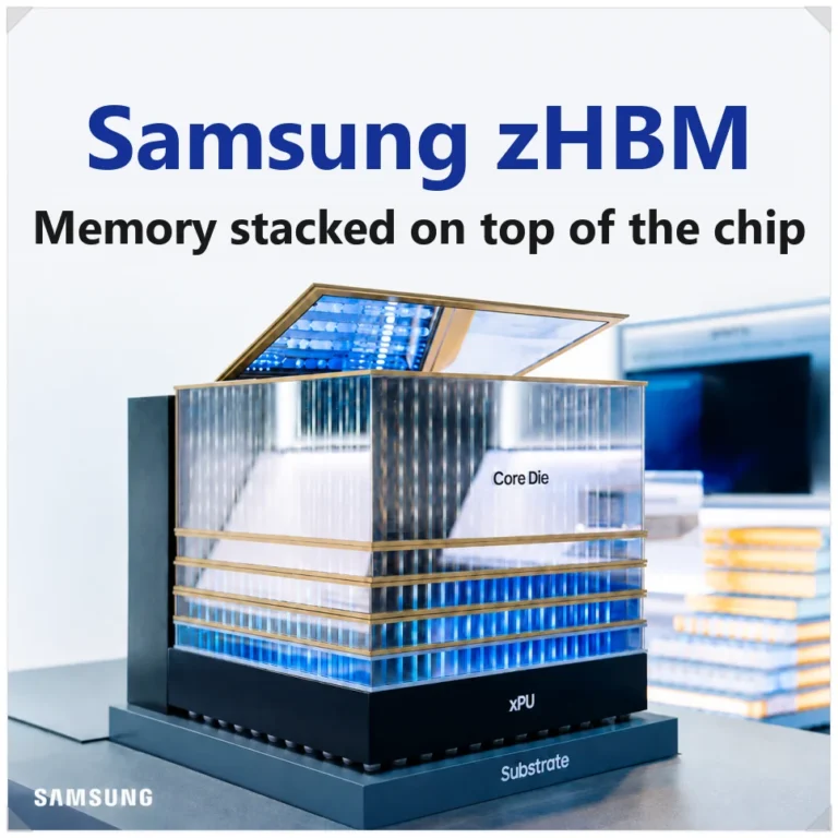
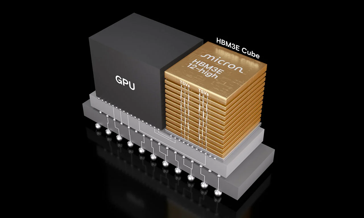
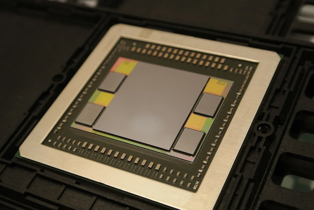
The fastest place for that data today is HBM, which sits right next to the GPU. But HBM stacks several memory dies in a complex package, which caps how much fits. It also costs far more per gigabyte than ordinary DDR5 DRAM.
Deleting old KV cache to save HBM has its own cost, because the context must be recomputed. In long conversations the same data gets processed again and again. Responses slow down and GPUs burn extra time.
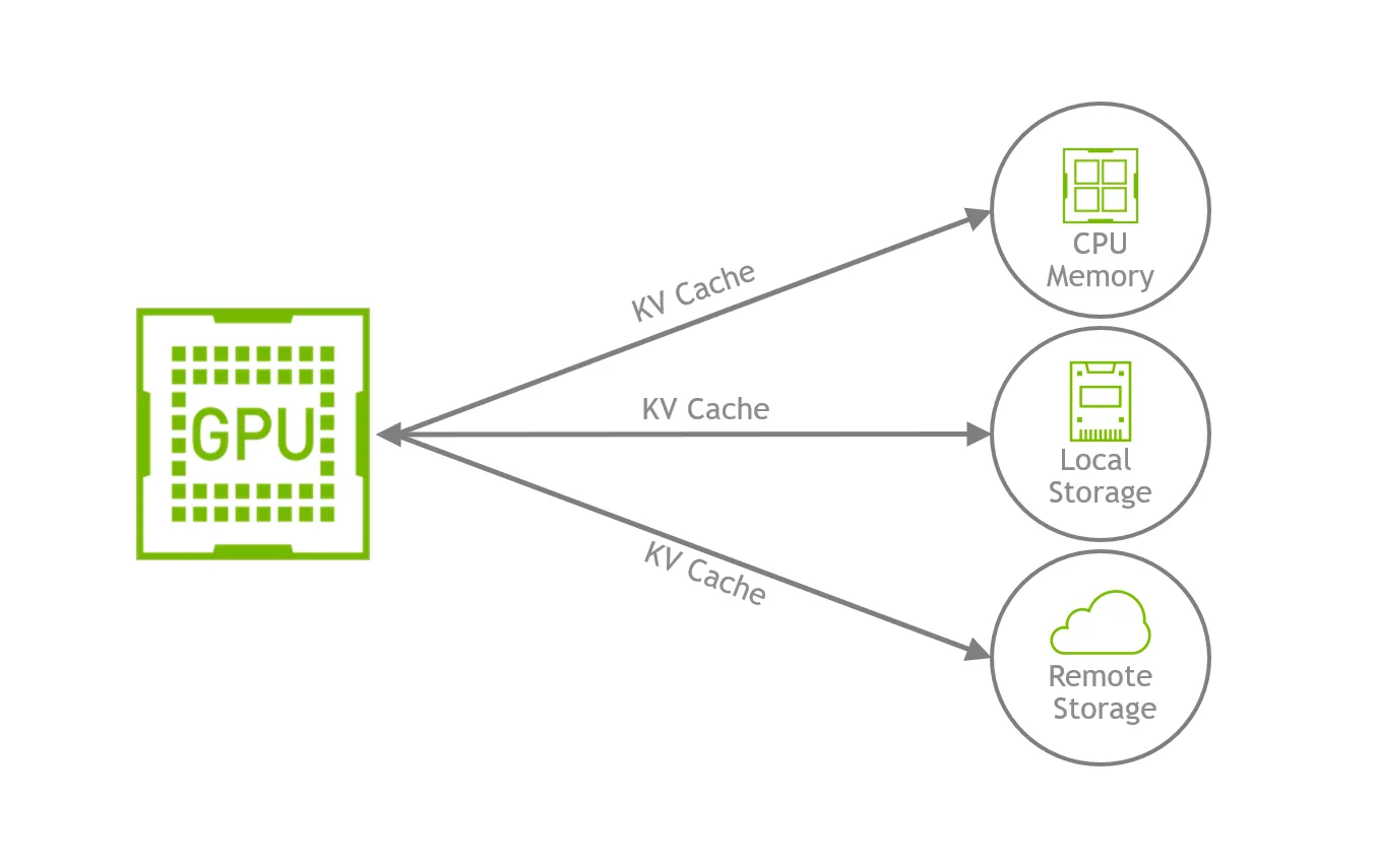
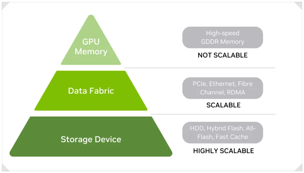
Operators can neither keep every context in HBM nor keep throwing cache away. The answer is to split AI inference memory into tiers and place data by how often and how urgently it is needed. HBF, CXL and CMX all build such tiers, but each stores and serves data in its own way.
How HBF eases HBM’s capacity limit
HBF (High Bandwidth Flash) stacks high-density NAND flash in layers to raise bandwidth and capacity together. It works alongside HBM as a new memory tier between HBM and ordinary SSDs. HBF stacks 3D NAND dies and connects each die’s I/O in parallel through TSVs (through-silicon vias). Individual NAND cells are slower than DRAM, but reaching many dies and channels at once raises total throughput.
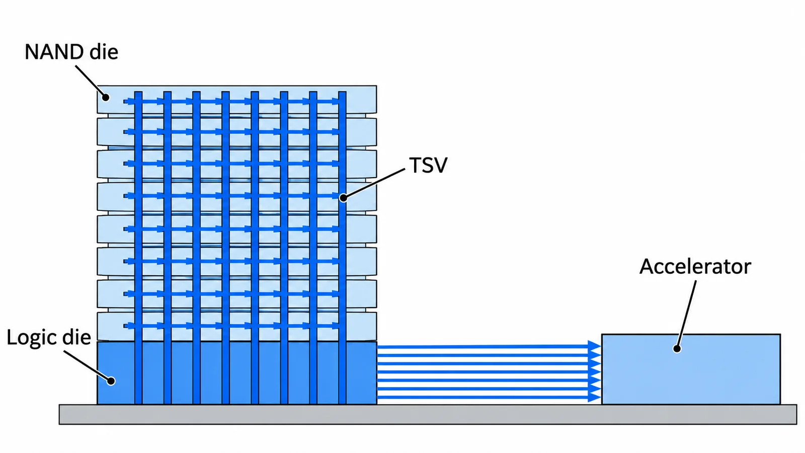
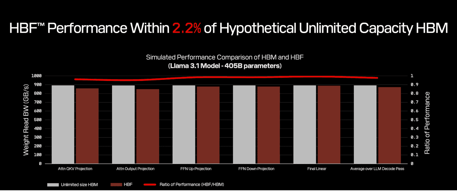
HBF is also non-volatile. DRAM loses its data when power is cut, while NAND keeps it. NAND also needs no periodic refresh, which helps cut idle power. Frequently used data can stay in HBM while less-accessed KV cache and model data move to HBF. Sandisk’s Llama 3.1 405B simulation put HBF within 2.2% of HBM with unlimited capacity.
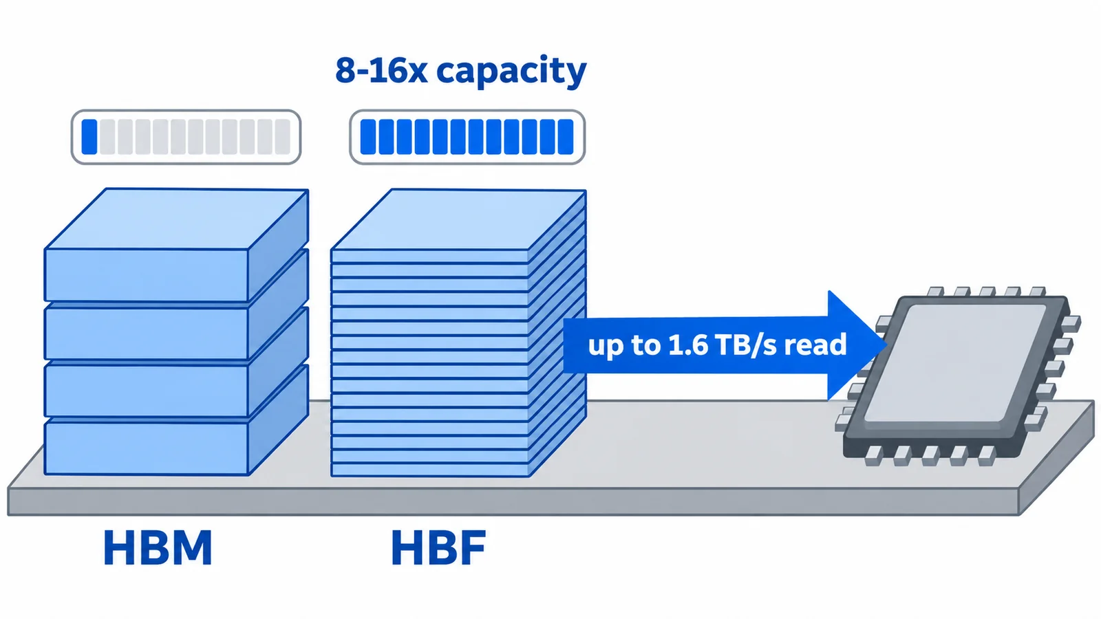
SK hynix and Sandisk are working together on HBF technology and its standardization. The first generation targets up to 1.6 TB/s of sequential read bandwidth from a single package. It is expected to offer roughly 8 to 16 times the capacity of HBM in the same footprint.
Sandisk and SK hynix released the first HBF technical specification through the Open Compute Project on Aug. 3, 2026, six months after the work began, with Google and Tenstorrent joining the consortium along the way.
HBF has not reached commercial products yet. Because it is NAND-based, it still has to solve write speed, endurance and the latency of random access. How it performs and holds up in real AI servers can only be judged once products ship.
How CXL memory pooling shares DRAM across servers
CXL (Compute Express Link) connects CPUs, GPUs and external memory devices at high speed. Instead of using only the memory installed in a server, a system can borrow memory attached to other devices when it needs it.
Enterprise servers are often fitted with more memory than they normally use to absorb sudden spikes. Yet memory makes up 30% to 40% of a server’s cost. So a lot of expensive capacity sits idle.
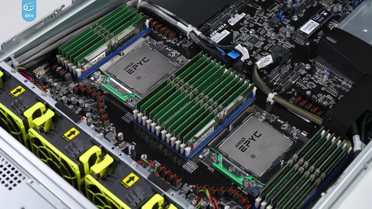
One server can run short while the server next to it has unused DRAM. The old architecture had no easy way to share it, so every server had to be fitted with expensive memory to spare.
CXL memory pooling creates a shared memory space that several servers can use. It assigns capacity to whichever CPU or GPU needs it. Microsoft’s Pond study found that CXL pooling reduces DRAM costs by 7%, with performance within 1% to 5% of local memory.
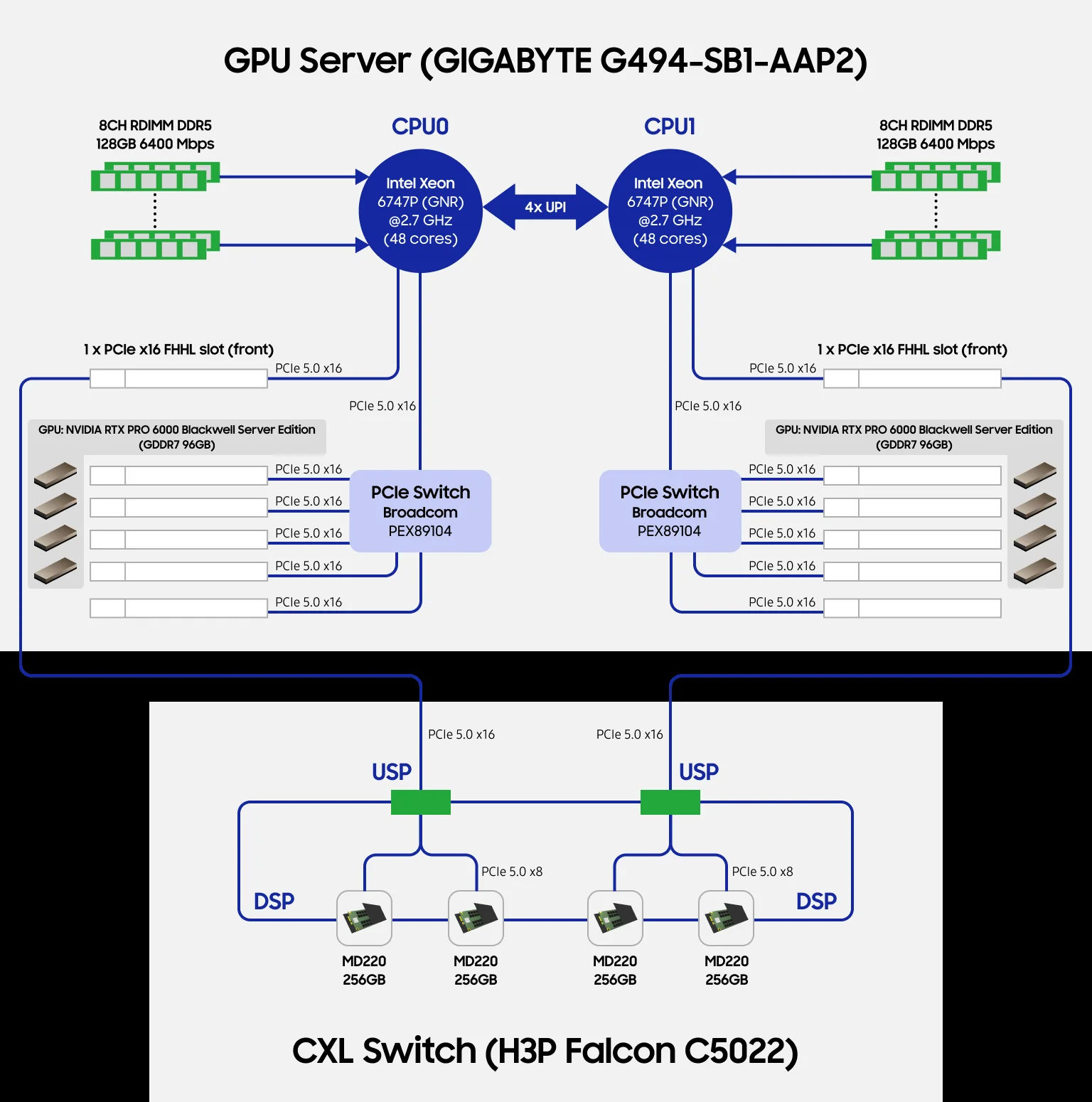
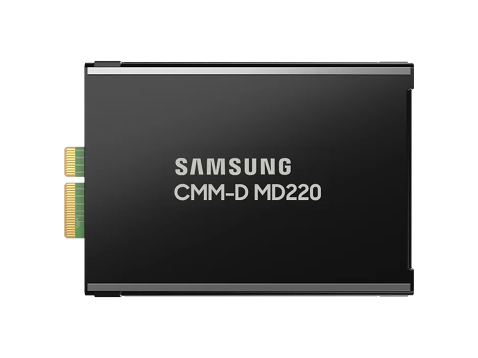
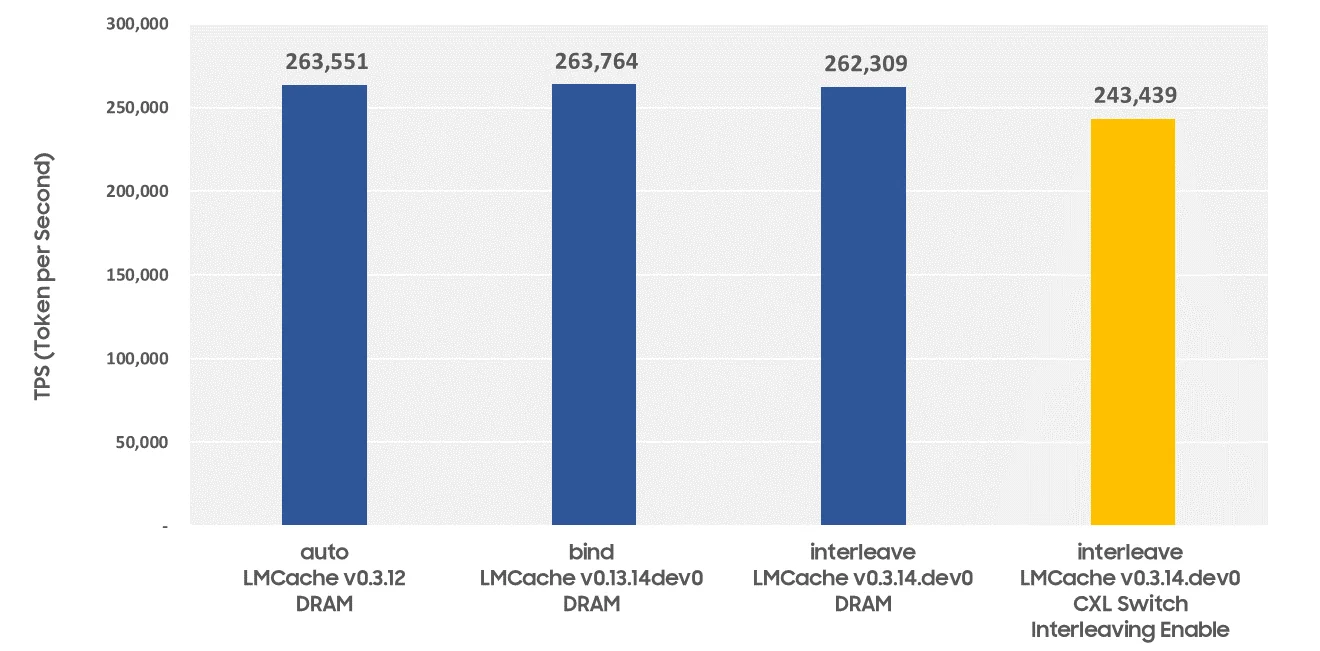
Samsung built a 1 TB memory pool by connecting NVIDIA Blackwell-based RTX PRO 6000 GPUs and its CMM-D memory modules through a CXL switch. Using LMCache, it stored the KV cache produced during inference in CXL memory. It measured the results in a June 2026 CMM-D white paper.
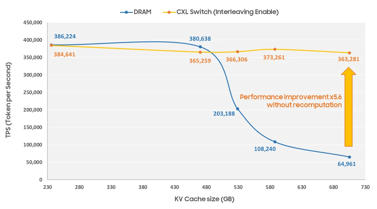
With one GPU, the CXL pool performed close to local DRAM. With eight GPUs pulling cache data at the same time, it still delivered about 92% of DRAM performance. The setup with only 512 GB of local DRAM ran out of room and had to delete some KV cache. When the same conversations continued, it recomputed the lost context. Both response speed and throughput fell.
The setup with the 1 TB CXL pool could move cache that did not fit in local DRAM out to external memory. As requests grew, it did not have to discard existing data and kept performance relatively stable.
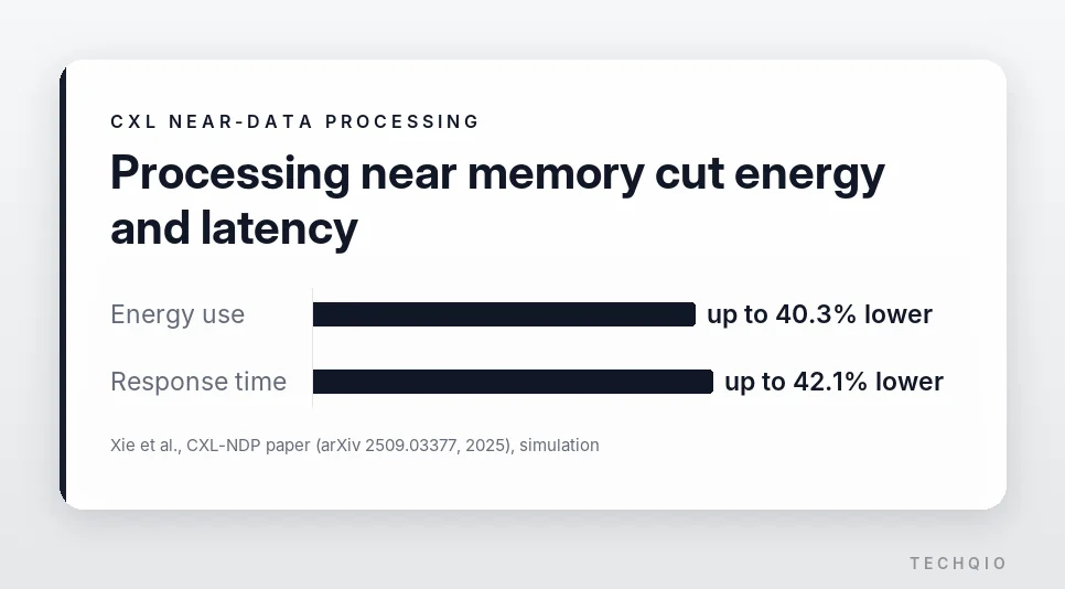
Because CXL memory sits outside the server, moving data adds latency. CXL-NDP (near-data processing) tackles this by handling simple tasks such as compression or conversion close to the memory. That shrinks the data sent to the CPU or GPU. In related tests, the needed logic fit in 5.7 mm² or less on a 7nm process, and energy use and response time improved by 40.3% and 42.1%, respectively.
CXL makes up for HBM’s limited capacity with memory from outside the server. Data being processed right now stays in HBM, while large, rarely used KV cache moves to CXL memory. That balances speed and cost.
NVIDIA CMX: a flash tier for long-lived context
NVIDIA introduced the CMX (Context Memory eXtension) architecture alongside its next-generation Rubin platform. It stores AI agents’ long conversation histories and context outside the GPU while still loading them quickly when needed. NVIDIA unveiled it at GTC as the CMX context memory storage platform. It is the first rack-scale implementation of BlueField-4 STX.
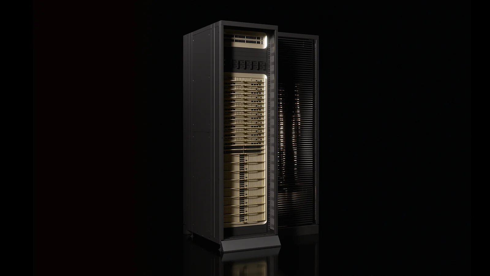
Until now, KV cache and session data that did not fit in HBM usually went to ordinary SSDs. That provided capacity, but pulling the data back to the GPU when a conversation resumed added delay.
CMX uses flash storage as a fast cache that takes part in AI inference. Data in use stays in HBM, while context that is idle but likely to be needed again goes to flash.
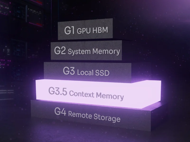
NVIDIA describes this as a G3.5 tier for KV cache. It is Ethernet-attached flash that sits below a node’s local SSDs (G3) and above shared remote storage (G4). GPU HBM (G1) and system memory (G2) sit on top.
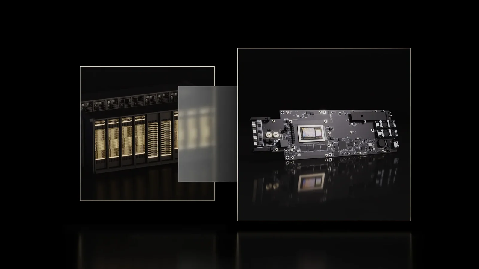
Data moves through BlueField-4 DPUs and the Spectrum-X network. The DPU takes over networking and data transfer from the CPU. It reaches flash in other servers directly over RDMA to cut latency. As a result, each GPU no longer depends only on its own VRAM. Flash spread across servers and racks can work as one large context store.
On the software side, NIXL and DOCA Memos handle data movement and context management. Dynamo orchestrates inference work. Combined with it, the system can check request queues and GPU state and pull likely-needed data into HBM ahead of time.
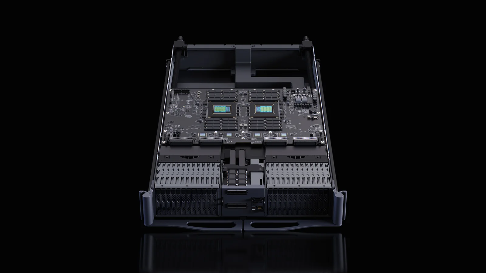
When those predictions are right, GPUs wait less and handle more requests in the same time. NVIDIA says CMX can improve token throughput and power efficiency by up to 5x each.
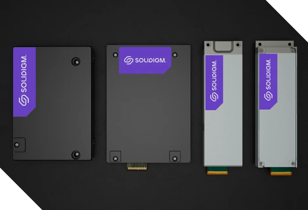
Solidigm has introduced the D7-PS1010 flash drive for the CMX fast-cache role. Its CMX guide calls the D7-PS1010 the preferred choice for latency-sensitive context workloads. Dell, HPE, Pure Storage and VAST Data are also preparing systems. Real performance will depend on cache hit rates, network design and how data is moved.
Prefetching data that is not needed wastes bandwidth, and missing data that is needed leaves GPUs waiting. In the end, CMX depends on the speed of the flash and, just as much, on the software that decides which context to move into HBM, and when.
Chipflation: AI demand pushes memory prices up
Fast-growing demand for AI infrastructure is pushing memory prices up. The effect reaches PCs and smartphones as well as servers. When rising chip prices lift the retail price of IT devices, it is called chipflation.
Global cloud companies are buying GPUs, HBM and high-capacity SSDs in bulk for AI data centers. Major memory makers are shifting toward more profitable HBM. That may leave less supply for mainstream DDR5 DRAM and NAND flash.
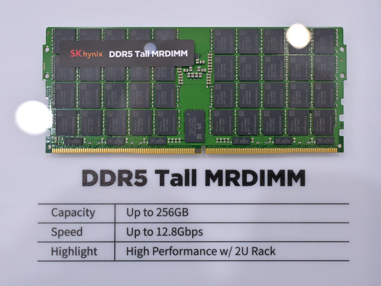
When AI memory absorbs capacity meant for everyday products, price pressure spreads to devices with no direct link to HBM.
It reaches down to the motherboards and storage that repair centers use as replacement parts. Gartner expects a 130% jump in combined DRAM and SSD prices by the end of 2026 to raise smartphone prices 13% and PC prices 17% over 2025, and Omdia forecasts the average smartphone selling price to rise 21% to $565 in 2026.
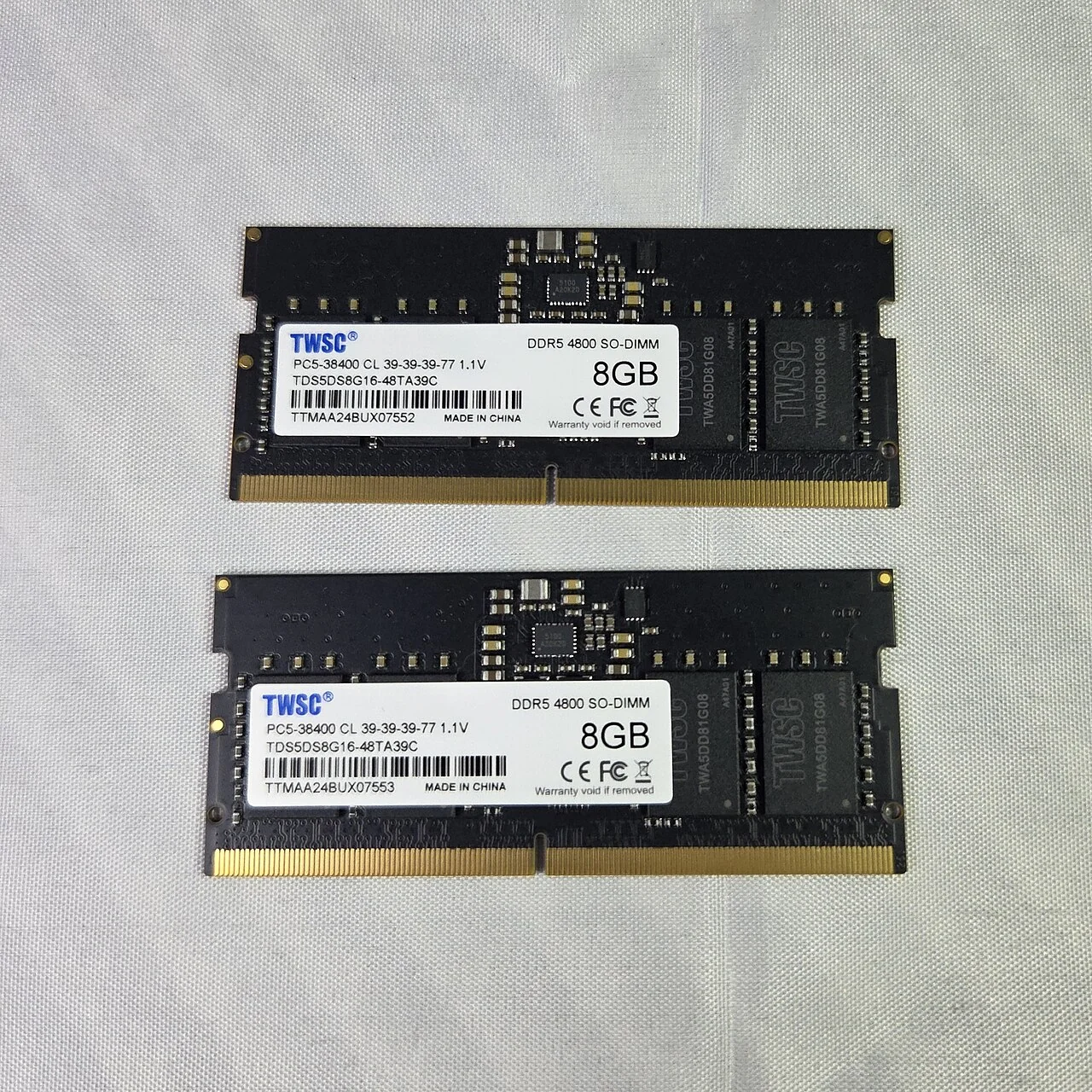
The industry is responding by expanding fabs and advanced packaging. SK hynix is adding capacity centered on its M15X fab in Cheongju and the Yongin semiconductor cluster. WSTS expects memory to account for a large share of the global chip market in 2026.
More supply does not make the bottleneck disappear. First the problem was getting GPUs, then it was HBM and advanced packaging capacity. Next, operators have to plan memory capacity for the whole rack along with networking, power delivery and cooling.
Where each kind of data should live
In the early AI build-out, the winner was whoever secured the most fast GPUs. As inference grows, what matters more is how efficiently GPUs and memory are arranged within a fixed budget and power envelope. Keeping all data in the fastest, most expensive HBM is simple, but it does not hold up once capacity and cost are counted.
Data in active use and frequently called KV cache belong in HBM. Data that must come back quickly can sit in HBF or CXL memory. Conversation histories and context that need to last longer can go to flash, with CMX moving them back into HBM when needed.
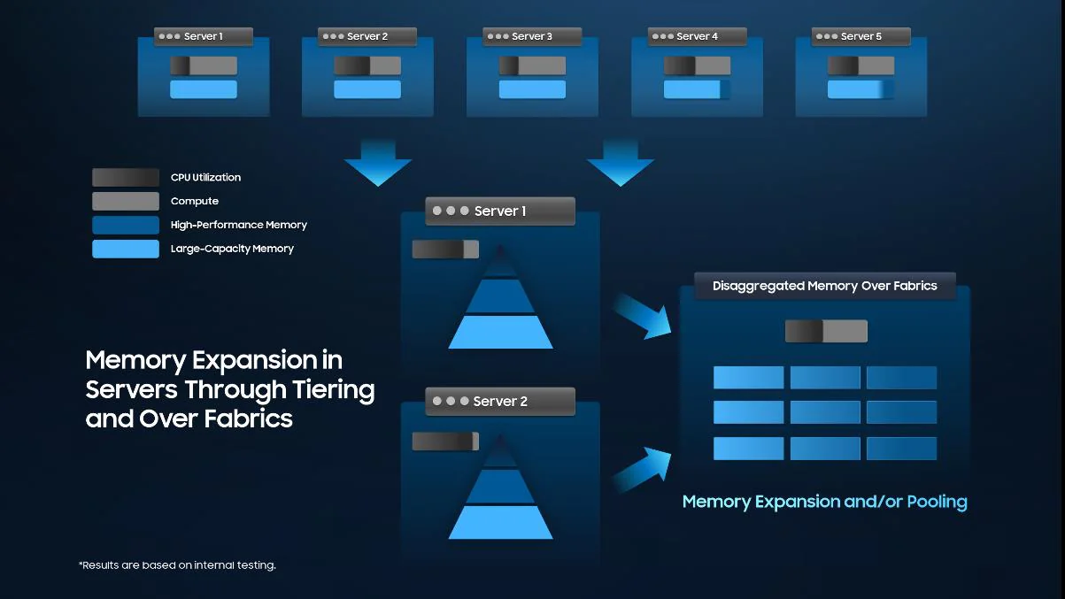
None of HBM, HBF, CXL and CMX fully replaces the others. HBM handles the data for the fastest computation, and HBF is strong at storing more data in the same space. CXL pools memory across servers to use it more efficiently, and CMX uses flash and the network to load large amounts of context quickly.
Because each differs in speed, capacity and price, data has to be placed by how often it is used. The software that decides what stays in HBM and what moves to HBF or CXL matters as much as the hardware. Misjudge when to move data, and needless copies and delays actually increase.
Installing as much of the fastest memory as possible does not by itself cut inference costs. The whole system has to be designed so the right data comes from the right tier at the right time. As AI models handle longer contexts and more users, how AI inference memory is tiered will be a key factor in data center performance and operating cost.
Related reading
- Why TSMC Teamed Up With GlobalFoundries: Silicon Interposers and CoWoS Explained
- CXMT 4F² DRAM: Can China’s New Memory Tech Really Threaten Samsung and SK Hynix?